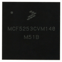
MCF5253CVM140 Freescale Semiconductor, MCF5253CVM140 Datasheet - Page 99

MCF5253CVM140
Manufacturer Part Number
MCF5253CVM140
Description
IC MPU 32BIT 140MHZ 225-MAPBGA
Manufacturer
Freescale Semiconductor
Series
MCF525xr
Datasheets
1.MCF5253VM140J.pdf
(34 pages)
2.MCF5253VM140J.pdf
(8 pages)
3.MCF5253VM140J.pdf
(648 pages)
4.MCF5253VM140J.pdf
(2 pages)
Specifications of MCF5253CVM140
Core Processor
Coldfire V2
Core Size
32-Bit
Speed
140MHz
Connectivity
CAN, EBI/EMI, I²C, QSPI, UART/USART, USB OTG
Peripherals
DMA, WDT
Program Memory Type
ROMless
Ram Size
128K x 8
Voltage - Supply (vcc/vdd)
1.08 V ~ 1.32 V
Data Converters
A/D 6x12b
Oscillator Type
External
Operating Temperature
-40°C ~ 85°C
Package / Case
225-MAPBGA
Family Name
MCF5xxx
Device Core
ColdFire V2
Device Core Size
32b
Frequency (max)
140MHz
Instruction Set Architecture
RISC
Supply Voltage 1 (typ)
1.2/3.3V
Operating Supply Voltage (max)
1.32/3.6V
Operating Supply Voltage (min)
1.08/3V
Operating Temp Range
-40C to 85C
Operating Temperature Classification
Industrial
Mounting
Surface Mount
Pin Count
225
Package Type
MA-BGA
Lead Free Status / RoHS Status
Lead free / RoHS Compliant
Number Of I /o
-
Eeprom Size
-
Program Memory Size
-
Lead Free Status / Rohs Status
Compliant
Available stocks
Company
Part Number
Manufacturer
Quantity
Price
Company:
Part Number:
MCF5253CVM140
Manufacturer:
FREESCALE
Quantity:
300
Company:
Part Number:
MCF5253CVM140
Manufacturer:
Freescale Semiconductor
Quantity:
10 000
Part Number:
MCF5253CVM140
Manufacturer:
FREESCALE
Quantity:
20 000
Company:
Part Number:
MCF5253CVM140J
Manufacturer:
Freescale Semiconductor
Quantity:
10 000
- MCF5253VM140J PDF datasheet
- MCF5253VM140J PDF datasheet #2
- MCF5253VM140J PDF datasheet #3
- MCF5253VM140J PDF datasheet #4
- Current page: 99 of 648
- Download datasheet (8Mb)
Chapter 6
Static RAM (SRAM)
This chapter describes the SRAM operation, memory map, register descriptions, initialization and SRAM
power management.
6.1
6.2
The SRAM module provides a general-purpose memory block that the ColdFire processor can access in a
single cycle. The location of the memory block can be specified to any modulo-64K address within the
4GB address space. The memory is ideal for storing critical code or data structures or for use as the system
stack. Because the SRAM module is physically connected to the processor's high-speed local bus.
Depending on configuration information, instruction fetches may be sent to both the cache and the SRAM
block simultaneously. If the reference is mapped into the region defined by the SRAM, the SRAM
provides the data back to the processor, and the cache data discarded. Accesses from the SRAM module
are not cached.
Only SRAM1 can be accessed by the DMA controller of the MCF5253. SRAM0 and SRAM1 are made
up of two memory arrays each consisting of 2048 lines, with 16 Bytes in each line.
As SRAM1 can be accessed by the DMA then the split in the array (Upper 32K bank and Lower 32K bank)
allows simultaneous access by both DMA and the CPU.
6.3
The SRAM programming model includes a description of the SRAM base address register (RAMBAR),
SRAM initialization, and power management.
6.3.1
The configuration information in the SRAM Base Address Register (RAMBAR[0:1]) controls the
operation of the SRAM module.
Freescale Semiconductor
•
•
•
•
•
•
Two 64 Kbyte SRAMS
Single-cycle access
Physically located on processor's high-speed local bus
Memory location programmable on any 64 Kbyte address boundary
Byte, word, longword address capabilities
There are 2 RAMBAR registers. One for SRAM0, the second for SRAM1.
SRAM Features
SRAM Operation
SRAM Memory Map and Register Definitions
SRAM Base Address Register
MCF5253 Reference Manual, Rev. 1
Figure 1-1
shows this concept.
6-1
Related parts for MCF5253CVM140
Image
Part Number
Description
Manufacturer
Datasheet
Request
R
Part Number:
Description:
Mcf5253 Coldfire? Microprocessor Data Sheet
Manufacturer:
Freescale Semiconductor, Inc
Datasheet:
Part Number:
Description:
Manufacturer:
Freescale Semiconductor, Inc
Datasheet:
Part Number:
Description:
Manufacturer:
Freescale Semiconductor, Inc
Datasheet:
Part Number:
Description:
Manufacturer:
Freescale Semiconductor, Inc
Datasheet:
Part Number:
Description:
Manufacturer:
Freescale Semiconductor, Inc
Datasheet:
Part Number:
Description:
Manufacturer:
Freescale Semiconductor, Inc
Datasheet:
Part Number:
Description:
Manufacturer:
Freescale Semiconductor, Inc
Datasheet:
Part Number:
Description:
Manufacturer:
Freescale Semiconductor, Inc
Datasheet:
Part Number:
Description:
Manufacturer:
Freescale Semiconductor, Inc
Datasheet:
Part Number:
Description:
Manufacturer:
Freescale Semiconductor, Inc
Datasheet:
Part Number:
Description:
Manufacturer:
Freescale Semiconductor, Inc
Datasheet:
Part Number:
Description:
Manufacturer:
Freescale Semiconductor, Inc
Datasheet:
Part Number:
Description:
Manufacturer:
Freescale Semiconductor, Inc
Datasheet:
Part Number:
Description:
Manufacturer:
Freescale Semiconductor, Inc
Datasheet:
Part Number:
Description:
Manufacturer:
Freescale Semiconductor, Inc
Datasheet:


