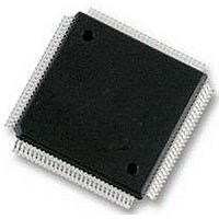
XC68HC12A0CPV8 Freescale Semiconductor, XC68HC12A0CPV8 Datasheet - Page 115

XC68HC12A0CPV8
Manufacturer Part Number
XC68HC12A0CPV8
Description
IC, 16BIT MCU, 68HC12, 8MHZ, TQFP-112
Manufacturer
Freescale Semiconductor
Datasheet
1.MC912D60ACFUE8.pdf
(460 pages)
Specifications of XC68HC12A0CPV8
Controller Family/series
68HC12
No. Of I/o's
68
Eeprom Memory Size
1KB
Ram Memory Size
2KB
Cpu Speed
8MHz
No. Of Timers
1
Core Size
16 Bit
Program Memory Size
60KB
Peripherals
ADC
Lead Free Status / RoHS Status
Lead free / RoHS Compliant
- Current page: 115 of 460
- Download datasheet (5Mb)
8.6 Program/Erase Operation
8.7 Shadow Word Mapping
MC68HC912D60A — Rev. 3.1
Freescale Semiconductor
A program or erase operation should follow the sequence below if AUTO
bit is clear:
If the AUTO bit is set, steps 4 and 5 can be replaced by a step to poll the
EEPGM bit until it is cleared.
It is possible to program/erase more bytes or words without intermediate
EEPROM reads, by jumping from step 5 to step 2.
The shadow word is mapped to location $_FC0 and $_FC1 when the
NOSHW bit in EEMCR register is zero. The value in the shadow word is
loaded to the EEMCR, EEDIVH and EEDIVL after reset.
shows the mapping of each bit from shadow word to the registers
1. Reserved for testing. Must be set to one in user application.
2. Reserved. Must be set to one in user application for future compatibility.
1. Write BYTE, ROW and ERASE to desired value, write EELAT = 1
2. Write a byte or an aligned word to an EEPROM address
3. Write EEPGM = 1
4. Wait for programming,
5. Write EEPGM = 0
6. Write EELAT = 0
Shadow word location
$_FC0, bit 3:2
$_FC0, bit 1:0
$_FC1, bit 7:0
$_FC0, bit 6
$_FC0, bit 5
$_FC0, bit 4
$_FC0 bit 7
EEPROM Memory
Table 8-4. Shadow word mapping
t
PROG
or erase,
t
ERASE
EEMCR / NOBDML
EEMCR / FPOPEN
EEDIVCLK / bit 7:0
EEMCR / NOSHW
EEMCR / bit 5
EEDIVH / bit 1:0
not mapped
Register / Bit
delay time (10ms)
Program/Erase Operation
EEPROM Memory
Table 8-4
(2)
(1)
Technical Data
115
Related parts for XC68HC12A0CPV8
Image
Part Number
Description
Manufacturer
Datasheet
Request
R
Part Number:
Description:
Manufacturer:
Freescale Semiconductor, Inc
Datasheet:
Part Number:
Description:
Manufacturer:
Freescale Semiconductor, Inc
Datasheet:
Part Number:
Description:
Manufacturer:
Freescale Semiconductor, Inc
Datasheet:
Part Number:
Description:
Manufacturer:
Freescale Semiconductor, Inc
Datasheet:
Part Number:
Description:
Manufacturer:
Freescale Semiconductor, Inc
Datasheet:
Part Number:
Description:
Manufacturer:
Freescale Semiconductor, Inc
Datasheet:
Part Number:
Description:
Manufacturer:
Freescale Semiconductor, Inc
Datasheet:
Part Number:
Description:
Manufacturer:
Freescale Semiconductor, Inc
Datasheet:
Part Number:
Description:
Manufacturer:
Freescale Semiconductor, Inc
Datasheet:
Part Number:
Description:
Manufacturer:
Freescale Semiconductor, Inc
Datasheet:
Part Number:
Description:
Manufacturer:
Freescale Semiconductor, Inc
Datasheet:
Part Number:
Description:
Manufacturer:
Freescale Semiconductor, Inc
Datasheet:
Part Number:
Description:
Manufacturer:
Freescale Semiconductor, Inc
Datasheet:
Part Number:
Description:
Manufacturer:
Freescale Semiconductor, Inc
Datasheet:
Part Number:
Description:
Manufacturer:
Freescale Semiconductor, Inc
Datasheet:


