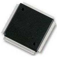
XC68HC12A0CPV8 Freescale Semiconductor, XC68HC12A0CPV8 Datasheet - Page 361

XC68HC12A0CPV8
Manufacturer Part Number
XC68HC12A0CPV8
Description
IC, 16BIT MCU, 68HC12, 8MHZ, TQFP-112
Manufacturer
Freescale Semiconductor
Datasheet
1.MC912D60ACFUE8.pdf
(460 pages)
Specifications of XC68HC12A0CPV8
Controller Family/series
68HC12
No. Of I/o's
68
Eeprom Memory Size
1KB
Ram Memory Size
2KB
Cpu Speed
8MHz
No. Of Timers
1
Core Size
16 Bit
Program Memory Size
60KB
Peripherals
ADC
Lead Free Status / RoHS Status
Lead free / RoHS Compliant
- Current page: 361 of 460
- Download datasheet (5Mb)
MC68HC912D60A — Rev. 3.1
Freescale Semiconductor
DJM — Result Register Data Justification Mode
exited, the ATD module powers up and continues operation. The
module is not reset; the register file is not reinitialized; the conversion
sequence is not restarted.
When the module comes out of wait, it is recommended that a
stabilization delay ( t
started.
For 10-bit resolution, left justified mode maps a result register into
data bus bits 6 through 15; bit 15 is the MSB. In right justified mode,
the result registers maps onto data bus bits 0 through 9; bit 9 is the
MSB.
For 8-bit resolution, left justified mode maps a result into the high byte
(bits 8 though 15; bit 15 is the MSB). Right justified maps a result into
the low byte (bits 0 through 7; bit 7 is the MSB).
Table 18-1
they are set up using the control bits.
Table 18-2
range between 0 and 5.1 Volts.
0 = Left justified mode
1 = Right justified mode
RES10
0
0
1
1
Analog-to-Digital Converter
Table 18-1. Result Data Formats Available
summarizes the result data formats available and how
illustrates left justified output codes for an input signal
DJM
0
1
0
1
SR
) is allowed before new conversions are
Description and Bus Bit Mapping
10-bit/left justified - bits 6-15
10-bit/right justified - bits 0-9
8-bit/left justified - bits 8-15
8-bit/right justified - bits 0-7
Result Data Formats
Analog-to-Digital Converter
Technical Data
ATD Registers
361
Related parts for XC68HC12A0CPV8
Image
Part Number
Description
Manufacturer
Datasheet
Request
R
Part Number:
Description:
Manufacturer:
Freescale Semiconductor, Inc
Datasheet:
Part Number:
Description:
Manufacturer:
Freescale Semiconductor, Inc
Datasheet:
Part Number:
Description:
Manufacturer:
Freescale Semiconductor, Inc
Datasheet:
Part Number:
Description:
Manufacturer:
Freescale Semiconductor, Inc
Datasheet:
Part Number:
Description:
Manufacturer:
Freescale Semiconductor, Inc
Datasheet:
Part Number:
Description:
Manufacturer:
Freescale Semiconductor, Inc
Datasheet:
Part Number:
Description:
Manufacturer:
Freescale Semiconductor, Inc
Datasheet:
Part Number:
Description:
Manufacturer:
Freescale Semiconductor, Inc
Datasheet:
Part Number:
Description:
Manufacturer:
Freescale Semiconductor, Inc
Datasheet:
Part Number:
Description:
Manufacturer:
Freescale Semiconductor, Inc
Datasheet:
Part Number:
Description:
Manufacturer:
Freescale Semiconductor, Inc
Datasheet:
Part Number:
Description:
Manufacturer:
Freescale Semiconductor, Inc
Datasheet:
Part Number:
Description:
Manufacturer:
Freescale Semiconductor, Inc
Datasheet:
Part Number:
Description:
Manufacturer:
Freescale Semiconductor, Inc
Datasheet:
Part Number:
Description:
Manufacturer:
Freescale Semiconductor, Inc
Datasheet:


