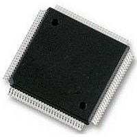
XC68HC12A0CPV8 Freescale Semiconductor, XC68HC12A0CPV8 Datasheet - Page 280

XC68HC12A0CPV8
Manufacturer Part Number
XC68HC12A0CPV8
Description
IC, 16BIT MCU, 68HC12, 8MHZ, TQFP-112
Manufacturer
Freescale Semiconductor
Datasheet
1.MC912D60ACFUE8.pdf
(460 pages)
Specifications of XC68HC12A0CPV8
Controller Family/series
68HC12
No. Of I/o's
68
Eeprom Memory Size
1KB
Ram Memory Size
2KB
Cpu Speed
8MHz
No. Of Timers
1
Core Size
16 Bit
Program Memory Size
60KB
Peripherals
ADC
Lead Free Status / RoHS Status
Lead free / RoHS Compliant
- Current page: 280 of 460
- Download datasheet (5Mb)
Multiple Serial Interface
15.5.4 Bidirectional Mode (MOMI or SISO)
15.5.5 Register Descriptions
SP0CR1 — SPI Control Register 1
Technical Data
280
RESET:
When SPE=1
Bidirectional
SPC0=0
SPC0=1
Normal
Mode
Mode
SPIE
Bit 7
0
SWOM enables open drain output. PS4 becomes GPIO.
Figure 15-6. Normal Mode and Bidirectional Mode
Serial Out
Serial Out
Serial In
Serial In
SPI
SPI
SPE
SWOM enables open drain output.
6
0
In bidirectional mode, the SPI uses only one serial data pin for external
device interface. The MSTR bit decides which pin to be used. The MOSI
pin becomes serial data I/O (MOMI) pin for the master mode, and the
MISO pin becomes serial data I/O (SISO) pin for the slave mode. The
direction of each serial I/O pin depends on the corresponding DDRS bit.
Control and data registers for the SPI subsystem are described below.
The memory address indicated for each register is the default address
that is in use after reset. For more information refer to
and Resource
Read or write anytime.
Master Mode
MSTR=1
DDS5
DDS5
SWOM
5
0
Multiple Serial Interface
Mapping.
MSTR
MOMI
4
0
PS4
MO
MI
CPOL
3
0
SWOM enables open drain output. PS5 becomes GPIO.
Serial Out
Serial Out
Serial In
Serial In
SPI
SPI
CPHA
SWOM enables open drain output.
2
1
Slave Mode
DDS4
DDS4
MSTR=0
SSOE
MC68HC912D60A — Rev. 3.1
1
0
Freescale Semiconductor
Operating Modes
LSBF
Bit 0
SISO
PS5
0
SO
SI
$00D0
Related parts for XC68HC12A0CPV8
Image
Part Number
Description
Manufacturer
Datasheet
Request
R
Part Number:
Description:
Manufacturer:
Freescale Semiconductor, Inc
Datasheet:
Part Number:
Description:
Manufacturer:
Freescale Semiconductor, Inc
Datasheet:
Part Number:
Description:
Manufacturer:
Freescale Semiconductor, Inc
Datasheet:
Part Number:
Description:
Manufacturer:
Freescale Semiconductor, Inc
Datasheet:
Part Number:
Description:
Manufacturer:
Freescale Semiconductor, Inc
Datasheet:
Part Number:
Description:
Manufacturer:
Freescale Semiconductor, Inc
Datasheet:
Part Number:
Description:
Manufacturer:
Freescale Semiconductor, Inc
Datasheet:
Part Number:
Description:
Manufacturer:
Freescale Semiconductor, Inc
Datasheet:
Part Number:
Description:
Manufacturer:
Freescale Semiconductor, Inc
Datasheet:
Part Number:
Description:
Manufacturer:
Freescale Semiconductor, Inc
Datasheet:
Part Number:
Description:
Manufacturer:
Freescale Semiconductor, Inc
Datasheet:
Part Number:
Description:
Manufacturer:
Freescale Semiconductor, Inc
Datasheet:
Part Number:
Description:
Manufacturer:
Freescale Semiconductor, Inc
Datasheet:
Part Number:
Description:
Manufacturer:
Freescale Semiconductor, Inc
Datasheet:
Part Number:
Description:
Manufacturer:
Freescale Semiconductor, Inc
Datasheet:


