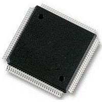
XC68HC12A0CPV8 Freescale Semiconductor, XC68HC12A0CPV8 Datasheet - Page 51

XC68HC12A0CPV8
Manufacturer Part Number
XC68HC12A0CPV8
Description
IC, 16BIT MCU, 68HC12, 8MHZ, TQFP-112
Manufacturer
Freescale Semiconductor
Datasheet
1.MC912D60ACFUE8.pdf
(460 pages)
Specifications of XC68HC12A0CPV8
Controller Family/series
68HC12
No. Of I/o's
68
Eeprom Memory Size
1KB
Ram Memory Size
2KB
Cpu Speed
8MHz
No. Of Timers
1
Core Size
16 Bit
Program Memory Size
60KB
Peripherals
ADC
Lead Free Status / RoHS Status
Lead free / RoHS Compliant
- Current page: 51 of 460
- Download datasheet (5Mb)
MC68HC912D60A — Rev. 3.1
Freescale Semiconductor
ADDR[15:8]
SMODN/BK
DATA[15:8]
ADDR[7:0]
GD/TAGHI
Pin Name
DATA[7:0]
CGMTST
PW[3:0]
LSTRB/
IPIPE1,
MODB/
MODA/
TAGLO
IPIPE0
ECLK
ECLK
XIRQ
DBE
SCK
CAL
R/W
IRQ
SS
80, 1–3
80-pin
23–16
48–41
26, 27
25
25
25
26
28
37
38
39
40
15
70
69
Pin Number
Table 3-2. MC68HC912D60A Signal Description Summary
112, 1–3
112-pin
31–24
64–57
37, 38
36
36
36
37
39
53
54
55
56
23
96
95
External bus pins share function with general-purpose I/O ports A and B.
Data bus control and, in expanded mode, enables the drive control of
Inverted ECLK used to latch the address.
CAL is the output of the Slow Mode programmable clock divider, SLWCLK,
Clock generation module test output.
State of mode select pins during reset determine the initial operating mode
E Clock is the output connection for the external bus clock. ECLK is used
Low byte strobe (0 = low byte valid), in all modes this pin can be used as
Indicates direction of data on expansion bus. Shares function with general-
Maskable interrupt request input provides a means of applying
Provides a means of requesting asynchronous nonmaskable interrupt
Single-wire background interface pin is dedicated to the background
Pulse Width Modulator channel outputs.
Slave select output for SPI master mode, input for slave mode or master
Serial clock for SPI system.
In single chip modes, the pins can be used for I/O. In expanded modes,
the pins are used for the external buses.
external buses during external reads.
and is used as a calibration reference for functions such as time of day. It
is overridden when DBE function is enabled. It always has a 50% duty
cycle.
of the MCU. After reset, MODB and MODA can be configured as
instruction queue tracking signals IPIPE1 and IPIPE0 or as general-
purpose I/O pins.
as a timing reference and for address demultiplexing.
I/O. The low strobe function is the exclusive-NOR of A0 and the internal
SZ8 signal. (The SZ8 internal signal indicates the size 16/8 access.) Pin
function TAGLO used in instruction tagging. See
purpose I/O. Read/write in expanded modes.
asynchronous interrupt requests to the MCU. Either falling edge-
sensitive triggering or level-sensitive triggering is program selectable
(INTCR register).
requests after reset initialization
debug function. During reset, this pin determines special or normal
operating mode. Pin function TAGHI used in instruction tagging. See
Development
mode.
Pinout and Signal Descriptions
Support.
Description
Pinout and Signal Descriptions
Development
Signal Descriptions
Technical Data
Support.
51
Related parts for XC68HC12A0CPV8
Image
Part Number
Description
Manufacturer
Datasheet
Request
R
Part Number:
Description:
Manufacturer:
Freescale Semiconductor, Inc
Datasheet:
Part Number:
Description:
Manufacturer:
Freescale Semiconductor, Inc
Datasheet:
Part Number:
Description:
Manufacturer:
Freescale Semiconductor, Inc
Datasheet:
Part Number:
Description:
Manufacturer:
Freescale Semiconductor, Inc
Datasheet:
Part Number:
Description:
Manufacturer:
Freescale Semiconductor, Inc
Datasheet:
Part Number:
Description:
Manufacturer:
Freescale Semiconductor, Inc
Datasheet:
Part Number:
Description:
Manufacturer:
Freescale Semiconductor, Inc
Datasheet:
Part Number:
Description:
Manufacturer:
Freescale Semiconductor, Inc
Datasheet:
Part Number:
Description:
Manufacturer:
Freescale Semiconductor, Inc
Datasheet:
Part Number:
Description:
Manufacturer:
Freescale Semiconductor, Inc
Datasheet:
Part Number:
Description:
Manufacturer:
Freescale Semiconductor, Inc
Datasheet:
Part Number:
Description:
Manufacturer:
Freescale Semiconductor, Inc
Datasheet:
Part Number:
Description:
Manufacturer:
Freescale Semiconductor, Inc
Datasheet:
Part Number:
Description:
Manufacturer:
Freescale Semiconductor, Inc
Datasheet:
Part Number:
Description:
Manufacturer:
Freescale Semiconductor, Inc
Datasheet:


