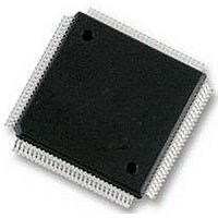
XC68HC12A0CPV8 Freescale Semiconductor, XC68HC12A0CPV8 Datasheet - Page 89

XC68HC12A0CPV8
Manufacturer Part Number
XC68HC12A0CPV8
Description
IC, 16BIT MCU, 68HC12, 8MHZ, TQFP-112
Manufacturer
Freescale Semiconductor
Datasheet
1.MC912D60ACFUE8.pdf
(460 pages)
Specifications of XC68HC12A0CPV8
Controller Family/series
68HC12
No. Of I/o's
68
Eeprom Memory Size
1KB
Ram Memory Size
2KB
Cpu Speed
8MHz
No. Of Timers
1
Core Size
16 Bit
Program Memory Size
60KB
Peripherals
ADC
Lead Free Status / RoHS Status
Lead free / RoHS Compliant
- Current page: 89 of 460
- Download datasheet (5Mb)
PORTE — Port E Register
DDRE — Port E Data Direction Register
MC68HC912D60A — Rev. 3.1
Freescale Semiconductor
RESET:
Function
RESET:
Alt. Pin
ECLK or
DDE7
DBE or
Bit 7
BIT 7
PE7
CAL
0
—
IPIPE1 or
CGMTST
MODB or
DDE6
PE6
6
0
—
6
This register is associated with external bus control signals and interrupt
inputs, including data bus enable (DBE), mode select (MODB/IPIPE1,
MODA/IPIPE0), ECLK, size (LSTRB), read/write (R/W), IRQ, and XIRQ.
When the associated pin is not used for one of these specific functions,
the pin can be used as general-purpose I/O. The port E assignment
register (PEAR) selects the function of each pin. DDRE determines the
primary direction of each port E pin when configured to be general-
purpose I/O.
Some of these pins have software selectable pull-ups (DBE, LSTRB,
R/W, IRQ, and XIRQ). A single control bit enables the pull-ups for all
these pins which are configured as inputs.
This register is not in the map in peripheral mode or expanded modes
when the EME bit is set.
Read and write anytime.
This register determines the primary direction for each port E pin
configured as general-purpose I/O.
MODA or
DDE5
IPIPE0
PE5
5
0
—
5
Bus Control and Input/Output
DDE4
ECLK
PE4
—
4
0
4
BDTAGL or
LSTRB or
TAGLO
DDE3
PE3
—
3
0
3
DDE2
PE2
R/W
—
2
0
2
PE1
IRQ
—
1
0
0
Bus Control and Input/Output
1
XIRQ
BIT 0
Bit 0
PE0
—
0
0
Technical Data
Registers
$0008
$0009
89
Related parts for XC68HC12A0CPV8
Image
Part Number
Description
Manufacturer
Datasheet
Request
R
Part Number:
Description:
Manufacturer:
Freescale Semiconductor, Inc
Datasheet:
Part Number:
Description:
Manufacturer:
Freescale Semiconductor, Inc
Datasheet:
Part Number:
Description:
Manufacturer:
Freescale Semiconductor, Inc
Datasheet:
Part Number:
Description:
Manufacturer:
Freescale Semiconductor, Inc
Datasheet:
Part Number:
Description:
Manufacturer:
Freescale Semiconductor, Inc
Datasheet:
Part Number:
Description:
Manufacturer:
Freescale Semiconductor, Inc
Datasheet:
Part Number:
Description:
Manufacturer:
Freescale Semiconductor, Inc
Datasheet:
Part Number:
Description:
Manufacturer:
Freescale Semiconductor, Inc
Datasheet:
Part Number:
Description:
Manufacturer:
Freescale Semiconductor, Inc
Datasheet:
Part Number:
Description:
Manufacturer:
Freescale Semiconductor, Inc
Datasheet:
Part Number:
Description:
Manufacturer:
Freescale Semiconductor, Inc
Datasheet:
Part Number:
Description:
Manufacturer:
Freescale Semiconductor, Inc
Datasheet:
Part Number:
Description:
Manufacturer:
Freescale Semiconductor, Inc
Datasheet:
Part Number:
Description:
Manufacturer:
Freescale Semiconductor, Inc
Datasheet:
Part Number:
Description:
Manufacturer:
Freescale Semiconductor, Inc
Datasheet:


