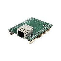
MOD5234-100IR NetBurner Inc, MOD5234-100IR Datasheet - Page 636
MOD5234-100IR
Manufacturer Part Number
MOD5234-100IR
Description
MOD5234 10/100 ETHERNET MODULE
Manufacturer
NetBurner Inc
Type
Controllers & Processorsr
Datasheets
1.MOD5272-100IR.pdf
(3 pages)
2.MOD5234-100IR.pdf
(4 pages)
3.MOD5234-100IR.pdf
(754 pages)
Specifications of MOD5234-100IR
Interface
I²C, SPI, UART
Voltage - Supply
2.5V
Mounting Type
Surface Mount
Package / Case
Module
Product
Modules
Lead Free Status / RoHS Status
Lead free / RoHS Compliant
Data Format
-
Baud Rates
-
Lead Free Status / Rohs Status
Lead free / RoHS Compliant
Other names
Q4483564


IEEE 1149.1 Test Access Port (JTAG)
31.2.2 Test Clock Input (TCLK)
The TCLK pin is a dedicated JTAG clock input to synchronize the test logic. Pulses on TCLK shift
data and instructions into the TDI pin on the rising edge and out of the TDO pin on the falling edge.
TCLK is independent of the processor clock. The TCLK pin has an internal pull-up resistor and
holding TCLK high or low for an indefinite period does not cause JTAG test logic to lose state
information.
31.2.3 Test Mode Select/Breakpoint (TMS/BKPT)
The TMS pin is the test mode select input that sequences the TAP state machine. TMS is sampled
on the rising edge of TCLK. The TMS pin has an internal pull-up resistor.
The BKPT pin is used to request an external breakpoint. Assertion of BKPT puts the processor into
a halted state after the current instruction completes.
31.2.4 Test Data Input/Development Serial Input (TDI/DSI)
The TDI pin receives serial test and data, which is sampled on the rising edge of TCLK. Register
values are shifted in least significant bit (lsb) first. The TDI pin has an internal pull-up resistor.
The DSI pin provides data input for the debug module serial communication port.
31.2.5 Test Reset/Development Serial Clock (TRST/DSCLK)
The TRST pin is an active low asynchronous reset input with an internal pull-up resistor that forces
the TAP controller to the test-logic-reset state.
The DSCLK pin clocks the serial communication port to the debug module. Maximum frequency
is 1/5 the processor clock speed. At the rising edge of DSCLK, the data input on DSI is sampled
and DSO changes state.
31-4
The JTAG_EN does not support dynamic switching between JTAG
and BDM modes.
Table 31-3. Signal State to the Disable Module
Disabling JTAG
Disabling BDM
MCF5235 Reference Manual, Rev. 2
JTAG_EN = 0
TRST = 0
TMS = 1
NOTE
—
Disable DSCLK
JTAG_EN = 1
BKPT = 1
DSI = 0
—
Freescale Semiconductor
Related parts for MOD5234-100IR
Image
Part Number
Description
Manufacturer
Datasheet
Request
R

Part Number:
Description:
MCU, MPU & DSP Development Tools MOD5234 MODULE
Manufacturer:
NetBurner Inc
Datasheet:

Part Number:
Description:
MCU, MPU & DSP Development Tools MOD5234 Core Module Development Kit
Manufacturer:
NetBurner Inc
Datasheet:

Part Number:
Description:
BOARD SERIAL-ETHERNET 512K FLASH
Manufacturer:
NetBurner Inc
Datasheet:

Part Number:
Description:
PROCESSOR MODULE FLASH MOD5272
Manufacturer:
NetBurner Inc
Datasheet:

Part Number:
Description:
PROCESSOR MODULE 512KB FLASH
Manufacturer:
NetBurner Inc
Datasheet:

Part Number:
Description:
DUAL PORT SERIAL-ETHERNET
Manufacturer:
NetBurner Inc
Datasheet:

Part Number:
Description:
PROCESSOR MODULE FLASH
Manufacturer:
NetBurner Inc
Datasheet:

Part Number:
Description:
PROCESSOR MODULE 512KB FLASH
Manufacturer:
NetBurner Inc
Datasheet:

Part Number:
Description:
KIT DEVELOP NETWORK FOR MOD5282
Manufacturer:
NetBurner Inc
Datasheet:

Part Number:
Description:
KIT DEVELOP NETWORK FOR MOD5272
Manufacturer:
NetBurner Inc
Datasheet:

Part Number:
Description:
DUAL PORT SERIAL-ETHERNET
Manufacturer:
NetBurner Inc
Datasheet:

Part Number:
Description:
Ethernet Modules & Development Tools 32 Bit 66MHz 40 Pin DIP Industrial Temp
Manufacturer:
NetBurner Inc
Datasheet:

Part Number:
Description:
Ethernet ICs 32bit 147MHz CAN-to- Ethnt Device IndTemp
Manufacturer:
NetBurner Inc
Datasheet: