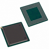
DS21Q55 Maxim Integrated Products, DS21Q55 Datasheet - Page 142

DS21Q55
Manufacturer Part Number
DS21Q55
Description
IC TXRX QUAD T1/E1/J1 SCT 256BGA
Manufacturer
Maxim Integrated Products
Datasheet
1.DS21Q55.pdf
(237 pages)
Specifications of DS21Q55
Function
Transceiver
Interface
E1, J1, T1
Number Of Circuits
4
Voltage - Supply
3.14 V ~ 3.47 V
Current - Supply
75mA
Operating Temperature
0°C ~ 70°C
Mounting Type
Surface Mount
Package / Case
256-BGA
Includes
BERT Generator and Detector, Dual HDLC Controllers
Lead Free Status / RoHS Status
Contains lead / RoHS non-compliant
Power (watts)
-
Available stocks
Company
Part Number
Manufacturer
Quantity
Price
Company:
Part Number:
DS21Q552
Manufacturer:
DALLAS
Quantity:
319
Company:
Part Number:
DS21Q552BN+
Manufacturer:
Maxim Integrated
Quantity:
10 000
Part Number:
DS21Q554
Manufacturer:
DALLAS
Quantity:
20 000
Part Number:
DS21Q554B+
Manufacturer:
MAXIM/美信
Quantity:
20 000
21.3.3 FIFO Information
The transmit FIFO buffer-available register indicates the number of bytes that can be written into the
transmit FIFO. The count form this register informs the host as to how many bytes can be written into the
transmit FIFO without overflowing the buffer.
Register Name:
Register Description:
Register Address:
Bit #
Name
Default
Bits 0 to 7/Transmit FIFO Bytes Available (TFBAO to TFBA7). TFBA0 is the LSB.
21.3.4 Receive Packet-Bytes Available
The lower 7 bits of the receive packet-bytes available register indicates the number of bytes (0 through
127) that can be read from the receive FIFO. The value indicated by this register (lower seven bits)
informs the host as to how many bytes can be read from the receive FIFO without going past the end of a
message. This value refers to one of four possibilities: the first part of a packet, the continuation of a
packet, the last part of a packet, or a complete packet. After reading the number of bytes indicated by this
register, the host then checks the HDLC information register for detailed message status.
If the value in the HxRPBA register refers to the beginning portion of a message or continuation of a
message, then the MSB of the HxRPBA register returns a value of 1. This indicates that the host can
safely read the number of bytes returned by the lower seven bits of the HxRPBA register, but there is no
need to check the information register since the packet has not yet terminated (successfully or otherwise).
Register Name:
Register Description:
Register Address:
Bit #
Name
Default
Bits 0 to 6/Receive FIFO Packet Bytes Available Count (RPBA0 to RPBA6). RPBA0 is the LSB.
Bit 7/Message Status (MS)
0 = bytes indicated by RPBA0 through RPBA6 are the end of a message. Host must check the INFO5 or
INFO6 register for details.
1 = bytes indicated by RPBA0 through RPBA6 are the beginning or continuation of a message. The host
does not need to check the INFO5 or INFO6 register.
TFBA7
MS
7
0
7
0
TFBA6
RPBA6
H1TFBA, H2TFBA
HDLC # 1 Transmit FIFO Buffer Available
HDLC # 2 Transmit FIFO Buffer Available
9Fh, Afh
H1RPBA, H2RPBA
HDLC # 1 Receive Packet Bytes Available
HDLC # 2 Receive Packet Bytes Available
9Ch, ACh
6
0
6
0
TFBA5
RPBA5
5
0
5
0
RPBA4
TFBA4
4
0
4
0
142 of 237
RPBA3
TFBA3
0
0
3
3
TFBA2
RPBA2
2
0
2
0
TFBA1
RPBA1
1
0
1
0
TFBA0
RPBA0
0
0
0
0


