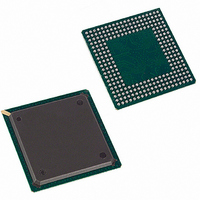
DS21Q55 Maxim Integrated Products, DS21Q55 Datasheet - Page 203

DS21Q55
Manufacturer Part Number
DS21Q55
Description
IC TXRX QUAD T1/E1/J1 SCT 256BGA
Manufacturer
Maxim Integrated Products
Datasheet
1.DS21Q55.pdf
(237 pages)
Specifications of DS21Q55
Function
Transceiver
Interface
E1, J1, T1
Number Of Circuits
4
Voltage - Supply
3.14 V ~ 3.47 V
Current - Supply
75mA
Operating Temperature
0°C ~ 70°C
Mounting Type
Surface Mount
Package / Case
256-BGA
Includes
BERT Generator and Detector, Dual HDLC Controllers
Lead Free Status / RoHS Status
Contains lead / RoHS non-compliant
Power (watts)
-
Available stocks
Company
Part Number
Manufacturer
Quantity
Price
Company:
Part Number:
DS21Q552
Manufacturer:
DALLAS
Quantity:
319
Company:
Part Number:
DS21Q552BN+
Manufacturer:
Maxim Integrated
Quantity:
10 000
Part Number:
DS21Q554
Manufacturer:
DALLAS
Quantity:
20 000
Part Number:
DS21Q554B+
Manufacturer:
MAXIM/美信
Quantity:
20 000
Table 30-B. ID Code Structure
Table 30-C. Device ID Codes
Note: When polling any single port on the DS21Q55,
30.3 Test Registers
IEEE 1149.1 requires a minimum of two test registers, the boundary scan register and the bypass register.
An optional test register, the identification register, has been included with the DS21Q55 design. It is
used with the IDCODE instruction and the Test-Logic-Reset state of the TAP controller.
30.4 Boundary Scan Register
This register contains both a shift register path and a latched parallel output for all control cells and digital
I/O cells. It is n bits in length. See
30.5 Bypass Register
This is a single one-bit shift register used with the BYPASS, CLAMP, and HIGH-Z instructions that
provides a short path between JTDI and JTDO.
30.6 Identification Register
The identification register contains a 32-bit shift register and a 32-bit latched parallel output. This register
is selected during the IDCODE instruction and when the TAP controller is in the Test-Logic-Reset state.
See
MSB
Version
Contact Factory
4 bits
Table 30-B
DS2155
DS2156
DS21354
DS21554
DS21352
DS21552
the device ID returned will be the DS2155 device ID.
PART
and
Device ID
16 bits
Table 30-C
16-BIT ID
0010h
0019h
0005h
0003h
0004h
0002h
JEDEC
00010100001
for more information on bit usage.
Table 30-D
for cell bit locations and definitions.
203 of 237
LSB
1
1


