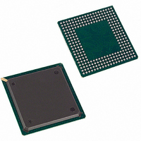
DS21Q55 Maxim Integrated Products, DS21Q55 Datasheet - Page 97

DS21Q55
Manufacturer Part Number
DS21Q55
Description
IC TXRX QUAD T1/E1/J1 SCT 256BGA
Manufacturer
Maxim Integrated Products
Datasheet
1.DS21Q55.pdf
(237 pages)
Specifications of DS21Q55
Function
Transceiver
Interface
E1, J1, T1
Number Of Circuits
4
Voltage - Supply
3.14 V ~ 3.47 V
Current - Supply
75mA
Operating Temperature
0°C ~ 70°C
Mounting Type
Surface Mount
Package / Case
256-BGA
Includes
BERT Generator and Detector, Dual HDLC Controllers
Lead Free Status / RoHS Status
Contains lead / RoHS non-compliant
Power (watts)
-
Available stocks
Company
Part Number
Manufacturer
Quantity
Price
Company:
Part Number:
DS21Q552
Manufacturer:
DALLAS
Quantity:
319
Company:
Part Number:
DS21Q552BN+
Manufacturer:
Maxim Integrated
Quantity:
10 000
Part Number:
DS21Q554
Manufacturer:
DALLAS
Quantity:
20 000
Part Number:
DS21Q554B+
Manufacturer:
MAXIM/美信
Quantity:
20 000
14.2.2 Software Signaling Insertion-Enable Registers, E1 CAS Mode
In E1 CAS mode, the CAS signaling alignment/alarm byte can be sourced from the transmit signaling
registers along with the signaling data.
Register Name:
Register Description:
Register Address:
Bit #
Name
Default
Bit 0/Upper CAS Align/Alarm Word (UCAW). Selects the upper CAS align/alarm pattern (0000) to be sourced
from the upper 4 bits of the TS1 register.
Bits 1 to 7/Software Signaling-Insertion Enable for Channels 1 to 7 (CH1 to CH7). These bits determine
which channels are to have signaling inserted from the transmit signaling registers.
Register Name:
Register Description:
Register Address:
Bit #
Name
Default
Bits 0 to 7/Software Signaling Insertion Enable for Channels 8 to 15 (CH8 to CH15). These bits determine
which channels are to have signaling inserted from the transmit signaling registers.
0 = do not source the upper CAS align/alarm pattern from the TS1 register
1 = source the upper CAS align/alarm pattern from the TS1 register
0 = do not source signaling data from the TSx registers for this channel
1 = source signaling data from the TSx registers for this channel
0 = do not source signaling data from the TSx registers for this channel
1 = source signaling data from the TSx registers for this channel
CH15
CH7
7
0
7
0
CH14
CH6
SSIE1
Software Signaling Insertion Enable 1
08h
SSIE2
Software Signaling Insertion Enable 2
09h
6
0
6
0
CH13
CH5
5
0
5
0
CH12
CH4
4
0
4
0
97 of 237
CH11
CH3
0
0
3
3
CH10
CH2
2
0
2
0
CH1
CH9
1
0
1
0
UCAW
CH8
0
0
0
0


