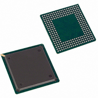
DS21Q55 Maxim Integrated Products, DS21Q55 Datasheet - Page 24

DS21Q55
Manufacturer Part Number
DS21Q55
Description
IC TXRX QUAD T1/E1/J1 SCT 256BGA
Manufacturer
Maxim Integrated Products
Datasheet
1.DS21Q55.pdf
(237 pages)
Specifications of DS21Q55
Function
Transceiver
Interface
E1, J1, T1
Number Of Circuits
4
Voltage - Supply
3.14 V ~ 3.47 V
Current - Supply
75mA
Operating Temperature
0°C ~ 70°C
Mounting Type
Surface Mount
Package / Case
256-BGA
Includes
BERT Generator and Detector, Dual HDLC Controllers
Lead Free Status / RoHS Status
Contains lead / RoHS non-compliant
Power (watts)
-
Available stocks
Company
Part Number
Manufacturer
Quantity
Price
Company:
Part Number:
DS21Q552
Manufacturer:
DALLAS
Quantity:
319
Company:
Part Number:
DS21Q552BN+
Manufacturer:
Maxim Integrated
Quantity:
10 000
Part Number:
DS21Q554
Manufacturer:
DALLAS
Quantity:
20 000
Part Number:
DS21Q554B+
Manufacturer:
MAXIM/美信
Quantity:
20 000
2.2 Parallel Control Port Pins
Signal Name:
Signal Description:
Signal Type:
Flags host controller during conditions and events defined in the status registers. Active-low, open-drain output.
Signal Name:
Signal Description:
Signal Type:
A dual function pin. A 0-to-1 transition issues a hardware reset to the DS21Q55 register set. A reset clears all
configuration registers. Configuration register contents are set to 0. Leaving TSTRST high tri-states all output and
I/O pins (including the parallel control port). Set low for normal operation. Useful in board-level testing.
Signal Name:
Signal Description:
Signal Type:
Set low to select nonmultiplexed bus operation. Set high to select multiplexed bus operation.
Signal Name:
Signal Description:
Signal Type:
In nonmultiplexed bus operation (MUX = 0), these serve as the data bus. In multiplexed bus operation (MUX = 1),
these pins serve as an 8-bit multiplexed address/data bus.
Signal Name:
Signal Description:
Signal Type:
In nonmultiplexed bus operation (MUX = 0), these serve as the address bus. In multiplexed bus operation
(MUX = 1), these pins are not used and should be connected low.
Signal Name:
Signal Description:
Signal Type:
Strap high to select Motorola bus timing; strap low to select Intel bus timing. This pin controls the function of the
RD (DS), ALE (AS), and WR (R/W) pins. If BTS = 1, then these pins assume the function listed in parentheses ().
Signal Name:
Signal Description:
Signal Type:
RD and DS are active-low signals. DS active HIGH when MUX = 1. See Bus Timing Diagrams.
INT
Interrupt
Output
TSTRST
Tri-State Control and Device Reset
Input
MUX
Bus Operation
Input
AD0 to AD7
Data Bus [D0 to D7] or Address/Data Bus
Input/Output
A0 to A6
Address Bus
Input
BTS
Bus Type Select
Input
RD (DS)
Read Input, Data Strobe
Input
24 of 237


