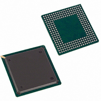
DS21Q55 Maxim Integrated Products, DS21Q55 Datasheet - Page 202

DS21Q55
Manufacturer Part Number
DS21Q55
Description
IC TXRX QUAD T1/E1/J1 SCT 256BGA
Manufacturer
Maxim Integrated Products
Datasheet
1.DS21Q55.pdf
(237 pages)
Specifications of DS21Q55
Function
Transceiver
Interface
E1, J1, T1
Number Of Circuits
4
Voltage - Supply
3.14 V ~ 3.47 V
Current - Supply
75mA
Operating Temperature
0°C ~ 70°C
Mounting Type
Surface Mount
Package / Case
256-BGA
Includes
BERT Generator and Detector, Dual HDLC Controllers
Lead Free Status / RoHS Status
Contains lead / RoHS non-compliant
Power (watts)
-
Available stocks
Company
Part Number
Manufacturer
Quantity
Price
Company:
Part Number:
DS21Q552
Manufacturer:
DALLAS
Quantity:
319
Company:
Part Number:
DS21Q552BN+
Manufacturer:
Maxim Integrated
Quantity:
10 000
Part Number:
DS21Q554
Manufacturer:
DALLAS
Quantity:
20 000
Part Number:
DS21Q554B+
Manufacturer:
MAXIM/美信
Quantity:
20 000
Table 30-A. Instruction Codes for IEEE 1149.1 Architecture
SAMPLE/PRELOAD
This is a mandatory instruction for the IEEE 1149.1 specification that supports two functions. The digital
I/Os of the device can be sampled at the boundary scan register without interfering with the normal
operation of the device by using the Capture-DR state. SAMPLE/PRELOAD also allows the device to
shift data into the boundary scan register through JTDI using the Shift-DR state.
BYPASS
When the BYPASS instruction is latched into the parallel instruction register, JTDI connects to JTDO
through the 1-bit bypass test register. This allows data to pass from JTDI to JTDO without affecting the
device’s normal operation.
EXTEST
This allows testing of all interconnections to the device. When the EXTEST instruction is latched in the
instruction register, the following actions occur: Once enabled through the Update-IR state, the parallel
outputs of all digital output pins are driven. The boundary scan register is connected between JTDI and
JTDO. The Capture-DR samples all digital inputs into the boundary scan register.
CLAMP
All digital outputs of the device output data from the boundary scan parallel output while connecting the
bypass register between JTDI and JTDO. The outputs do not change during the CLAMP instruction.
HIGHZ
All digital outputs of the device are placed in a high-impedance state. The BYPASS register is connected
between JTDI and JTDO.
IDCODE
When the IDCODE instruction is latched into the parallel instruction register, the identification test
register is selected. The device identification code is loaded into the identification register on the rising
edge of JTCLK following entry into the Capture-DR state. Shift-DR can be used to shift the identification
code out serially through JTDO. During Test-Logic-Reset, the identification code is forced into the
instruction register’s parallel output. The ID code always has a 1 in the LSB position. The next 11 bits
identify the manufacturer’s JEDEC number and number of continuation bytes followed by 16 bits for the
device and 4 bits for the version
SAMPLE/PRELOAD
INSTRUCTION
BYPASS
EXTEST
IDCODE
CLAMP
HIGHZ
SELECTED REGISTER
Device Identification
Boundary Scan
Boundary Scan
(Table
Bypass
Bypass
Bypass
30-B).
Table 30-C
202 of 237
INSTRUCTION CODES
lists the device ID codes for the SCT devices.
010
111
000
011
100
001


