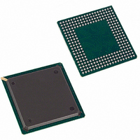
DS21Q55 Maxim Integrated Products, DS21Q55 Datasheet - Page 75

DS21Q55
Manufacturer Part Number
DS21Q55
Description
IC TXRX QUAD T1/E1/J1 SCT 256BGA
Manufacturer
Maxim Integrated Products
Datasheet
1.DS21Q55.pdf
(237 pages)
Specifications of DS21Q55
Function
Transceiver
Interface
E1, J1, T1
Number Of Circuits
4
Voltage - Supply
3.14 V ~ 3.47 V
Current - Supply
75mA
Operating Temperature
0°C ~ 70°C
Mounting Type
Surface Mount
Package / Case
256-BGA
Includes
BERT Generator and Detector, Dual HDLC Controllers
Lead Free Status / RoHS Status
Contains lead / RoHS non-compliant
Power (watts)
-
Available stocks
Company
Part Number
Manufacturer
Quantity
Price
Company:
Part Number:
DS21Q552
Manufacturer:
DALLAS
Quantity:
319
Company:
Part Number:
DS21Q552BN+
Manufacturer:
Maxim Integrated
Quantity:
10 000
Part Number:
DS21Q554
Manufacturer:
DALLAS
Quantity:
20 000
Part Number:
DS21Q554B+
Manufacturer:
MAXIM/美信
Quantity:
20 000
11.
Register Name:
Register Description:
Register Address:
Bit #
Name
Default
Bit 0/Framer Loopback (FLB). This loopback is useful in testing and debugging applications. In FLB, the device
loops data from the transmit side back to the receive side. When FLB is enabled, the following occurs:
1)
2)
3)
Bit 1/Payload Loopback (PLB). When PLB is enabled, the following occurs:
1)
2)
3)
4)
Bit 2/Remote Loopback (RLB). In this loopback, data input by the RPOSI and RNEGI pins is transmitted back to
the TPOSO and TNEGO pins. Data continues to pass through the receive-side framer of the device as it would
normally. Data from the transmit-side formatter is ignored. See
T1 Mode: An unframed all-ones code is transmitted at TPOSO and TNEGO.
E1 Mode: Normal data is transmitted at TPOSO and TNEGO.
Data at RPOSI and RNEGI is ignored.
All receive-side signals take on timing synchronous with TCLK instead of RCLKI.
Data is transmitted from the TPOSO and TNEGO pins synchronous with RCLK instead of TCLK.
All the receive side signals continue to operate normally.
Data at the TSER, TDATA, and TSIG pins is ignored.
The TLCLK signal becomes synchronous with RCLK instead of TCLK.
LOOPBACK CONFIGURATION
Please note that it is not acceptable to have RCLK connected to TCLK during this loopback because this
causes an unstable condition.
0 = loopback disabled
1 = loopback enabled
0 = loopback disabled
1 = loopback enabled
T1 Mode. Normally, this loopback is only enabled when ESF framing is being performed but can also be
enabled in D4 framing applications. In a PLB situation, the device loops the 192 bits of payload data (with
BPVs corrected) from the receive section back to the transmit section. The FPS framing pattern, CRC6
calculation, and the FDL bits are not looped back; they are reinserted by the device.
E1 Mode. In a PLB situation, the device loops the 248 bits of payload data (with BPVs corrected) from the
receive section back to the transmit section. The transmit section modifies the payload as if it was input at
TSER. The FAS word; Si, Sa, and E bits; and CRC4 are not looped back; they are reinserted by the device.
0 = loopback disabled
1 = loopback enabled
—
7
0
—
LBCR
Loopback Control Register
4Ah
6
0
—
5
0
LIUC
4
0
75 of 237
LLB
0
3
Figure 1-1
RLB
2
0
for more details.
PLB
1
0
FLB
0
0


