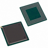
DS21Q55 Maxim Integrated Products, DS21Q55 Datasheet - Page 36

DS21Q55
Manufacturer Part Number
DS21Q55
Description
IC TXRX QUAD T1/E1/J1 SCT 256BGA
Manufacturer
Maxim Integrated Products
Datasheet
1.DS21Q55.pdf
(237 pages)
Specifications of DS21Q55
Function
Transceiver
Interface
E1, J1, T1
Number Of Circuits
4
Voltage - Supply
3.14 V ~ 3.47 V
Current - Supply
75mA
Operating Temperature
0°C ~ 70°C
Mounting Type
Surface Mount
Package / Case
256-BGA
Includes
BERT Generator and Detector, Dual HDLC Controllers
Lead Free Status / RoHS Status
Contains lead / RoHS non-compliant
Power (watts)
-
Available stocks
Company
Part Number
Manufacturer
Quantity
Price
Company:
Part Number:
DS21Q552
Manufacturer:
DALLAS
Quantity:
319
Company:
Part Number:
DS21Q552BN+
Manufacturer:
Maxim Integrated
Quantity:
10 000
Part Number:
DS21Q554
Manufacturer:
DALLAS
Quantity:
20 000
Part Number:
DS21Q554B+
Manufacturer:
MAXIM/美信
Quantity:
20 000
3. PARALLEL PORT
The DS21Q55 is controlled via a nonmultiplexed (MUX = 0) or a multiplexed (MUX = 1) bus by an
external microcontroller or microprocessor. The DS21Q55 can operate with either Intel or Motorola bus
timing configurations. If the BTS pin is tied low, Intel timing will be selected; if tied high, Motorola
timing will be selected. All Motorola bus signals are listed in parentheses (). See the timing diagrams in
the AC Electrical Characteristics for more details. Each of the four transceivers has a complete register
set as shown below. There are four individual chip-select signals (CS1, CS2, CS3, CS4) that are used
select one of the four transceivers.
3.1 Register Map
Table 3-A. Register Map Sorted by Address
ADDRESS
0A
0B
0C
0D
1A
1B
1C
1D
0E
0F
1E
1F
00
01
02
03
04
05
06
07
08
09
10
11
12
13
14
15
16
17
18
19
Master Mode Register
I/O Configuration Register 1
I/O Configuration Register 2
T1 Receive Control Register 1
T1 Receive Control Register 2
T1 Transmit Control Register 1
T1 Transmit Control Register 2
T1 Common Control Register 1
Software Signaling Insertion Enable 1
Software Signaling Insertion Enable 2
Software Signaling Insertion Enable 3
Software Signaling Insertion Enable 4
T1 Receive Digital Milliwatt Enable Register 1
T1 Receive Digital Milliwatt Enable Register 2
T1 Receive Digital Milliwatt Enable Register 3
Device Identification Register
Information Register 1
Information Register 2
Information Register 3
Reserved
Interrupt Information Register 1
Interrupt Information Register 2
Status Register 1
Interrupt Mask Register 1
Status Register 2
Interrupt Mask Register 2
Status Register 3
Interrupt Mask Register 3
Status Register 4
Interrupt Mask Register 4
Status Register 5
Interrupt Mask Register 5
REGISTER NAME
36 of 237
ABBREVIATION
REGISTER
MSTRREG
T1RDMR1
T1RDMR2
T1RDMR3
T1RCR1
T1RCR2
T1TCR1
T1TCR2
T1CCR1
IOCR1
IOCR2
INFO1
INFO2
INFO3
SSIE1
SSIE2
SSIE3
SSIE4
IMR1
IMR2
IMR3
IMR4
IMR5
IIR1
IIR2
IDR
SR1
SR2
SR3
SR4
SR5
—
PAGE
157
158
159
110
110
73
74
52
53
54
67
69
71
46
50
51
97
97
98
98
56
56
56
67
57
64
—
48
48
68
70
72


