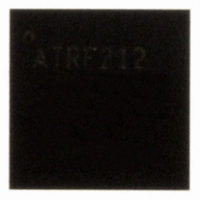
AT86RF212-ZU Atmel, AT86RF212-ZU Datasheet - Page 127

AT86RF212-ZU
Manufacturer Part Number
AT86RF212-ZU
Description
IC TXRX ZIGBE/802.15.4/ISM 32QFN
Manufacturer
Atmel
Datasheet
1.AT86RF212-ZU.pdf
(172 pages)
Specifications of AT86RF212-ZU
Frequency
700MHz, 800MHz, 900MHz
Data Rate - Maximum
250kbps
Modulation Or Protocol
802.15.4 Zigbee, 6LoWPAN, ISM
Applications
ISM, ZigBee™
Power - Output
10dBm
Sensitivity
-110dBm
Voltage - Supply
1.8 V ~ 3.6 V
Current - Receiving
9.2mA
Current - Transmitting
25mA
Data Interface
PCB, Surface Mount
Antenna Connector
PCB, Surface Mount
Operating Temperature
-40°C ~ 85°C
Package / Case
32-VQFN Exposed Pad, 32-HVQFN, 32-SQFN, 32-DHVQFN
Number Of Receivers
1
Number Of Transmitters
1
Wireless Frequency
769 MHz to 935 MHz
Interface Type
SPI
Noise Figure
7 dB
Output Power
21 dB
Operating Supply Voltage
1.8 V, 3 V
Maximum Operating Temperature
+ 85 C
Mounting Style
SMD/SMT
Maximum Supply Current
25 mA
Minimum Operating Temperature
- 40 C
Modulation
OQPSK
Protocol Supported
802.15.4
Operating Temperature (min)
-40C
Operating Temperature (max)
85C
Operating Temperature Classification
Industrial
Lead Free Status / RoHS Status
Lead free / RoHS Compliant
Memory Size
-
Lead Free Status / Rohs Status
Lead free / RoHS Compliant
Available stocks
Company
Part Number
Manufacturer
Quantity
Price
Company:
Part Number:
AT86RF212-ZU
Manufacturer:
HITTITE
Quantity:
5 000
Part Number:
AT86RF212-ZU
Manufacturer:
ATMEL/爱特梅尔
Quantity:
20 000
Part Number:
AT86RF212-ZUR
Manufacturer:
MICROCHIP/微芯
Quantity:
20 000
8168C-MCU Wireless-02/10
Register 0x1A (PLL_CF):
This register controls the operation of the center frequency calibration loop.
Table 7-40. Register 0x1A (PLL_CF)
• Bit 7 – PLL_CF_START
PLL_CF_START = 1 initiates the center frequency calibration. When the calibration
cycle has finished after at most 25 µs, the register bit PLL_CF_START is reset to 0.
• Bit 6:5
These bits are reserved and must always be written back using the reset values.
• Bit 4:0 – PLL_CF
Bits 4:0 represent the current CF state of the PLL. In order to assure the shortest
possible calibration time, they should not be changed when starting center frequency
tuning.
Register 0x1B (PLL_DCU):
This register controls the operation of the delay cell calibration loop.
Table 7-41. Register 0x1B (PLL_DCU)
• Bit 7 – PLL_DCU_START
PLL_DCU_START = 1 initiates the delay cell calibration. The calibration cycle is
completed after 10 µs and the register bit PLL_DCU_START is set to 0. The register bit
is cleared immediately after finishing the calibration.
• Bit 6:0 – Reserved
Bit
Name
Read/Write
Reset Value
Bit
Name
Read/Write
Reset Value
Bit
Name
Read/Write
Reset Value
Bit
Name
Read/Write
Reset Value
7
PLL_CF_START
R/W
0
3
PLL_CF[3]
R/W
1
7
PLL_DCU_START
R/W
0
3
Reserved
R/W
0
6
Reserved
R/W
1
2
PLL_CF[2]
R/W
0
6
Reserved
R/W
1
2
Reserved
R/W
0
5
Reserved
R/W
0
1
PLL_CF[1]
R/W
0
5
Reserved
R/W
0
1
Reserved
R/W
0
AT86RF212
4
PLL_CF[4]
R/W
0
0
PLL_CF[0]
R/W
0
4
Reserved
R/W
0
0
Reserved
R/W
0
127


