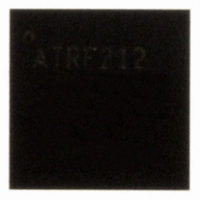
AT86RF212-ZU Atmel, AT86RF212-ZU Datasheet - Page 32

AT86RF212-ZU
Manufacturer Part Number
AT86RF212-ZU
Description
IC TXRX ZIGBE/802.15.4/ISM 32QFN
Manufacturer
Atmel
Datasheet
1.AT86RF212-ZU.pdf
(172 pages)
Specifications of AT86RF212-ZU
Frequency
700MHz, 800MHz, 900MHz
Data Rate - Maximum
250kbps
Modulation Or Protocol
802.15.4 Zigbee, 6LoWPAN, ISM
Applications
ISM, ZigBee™
Power - Output
10dBm
Sensitivity
-110dBm
Voltage - Supply
1.8 V ~ 3.6 V
Current - Receiving
9.2mA
Current - Transmitting
25mA
Data Interface
PCB, Surface Mount
Antenna Connector
PCB, Surface Mount
Operating Temperature
-40°C ~ 85°C
Package / Case
32-VQFN Exposed Pad, 32-HVQFN, 32-SQFN, 32-DHVQFN
Number Of Receivers
1
Number Of Transmitters
1
Wireless Frequency
769 MHz to 935 MHz
Interface Type
SPI
Noise Figure
7 dB
Output Power
21 dB
Operating Supply Voltage
1.8 V, 3 V
Maximum Operating Temperature
+ 85 C
Mounting Style
SMD/SMT
Maximum Supply Current
25 mA
Minimum Operating Temperature
- 40 C
Modulation
OQPSK
Protocol Supported
802.15.4
Operating Temperature (min)
-40C
Operating Temperature (max)
85C
Operating Temperature Classification
Industrial
Lead Free Status / RoHS Status
Lead free / RoHS Compliant
Memory Size
-
Lead Free Status / Rohs Status
Lead free / RoHS Compliant
Available stocks
Company
Part Number
Manufacturer
Quantity
Price
Company:
Part Number:
AT86RF212-ZU
Manufacturer:
HITTITE
Quantity:
5 000
Part Number:
AT86RF212-ZU
Manufacturer:
ATMEL/爱特梅尔
Quantity:
20 000
Part Number:
AT86RF212-ZUR
Manufacturer:
MICROCHIP/微芯
Quantity:
20 000
5.1.2.2 SLEEP – Sleep State
5.1.2.3 TRX_OFF – Clock State
32
AT86RF212
after power-on or reset. The input pull-up and pull-down resistors are disabled when the
radio transceiver leaves P_ON state. Leaving P_ON state, outputs pins DIG1/DIG2 are
internally connected to digital ground, whereas pins DIG3/DIG4 are internally connected
to analog ground, unless their configuration is changed. A reset at pin 8 (/RST) does
not enable the pull-up or pull-down resistors.
Prior to leaving P_ON, the microcontroller must set the input pins to the default
operating values: SLP_TR = L, /RST = H, and /SEL = H.
All interrupts are disabled by default. Thus, interrupts for state transition control are to
be enabled first, e.g. enable IRQ_4 (AWAKE_END) to indicate a state transition to
TRX_OFF state. In P_ON state, a first access to the radio transceiver registers is
possible after a default 1 MHz master clock is provided at pin 17 (CLKM), refer to t
Table 5-1.
Once the supply voltage has stabilized and the crystal oscillator has settled (see t
Table 5-2), the interrupt mask for the AWAKE_END should be set. A valid SPI write
access to register bits TRX_CMD (register 0x02, TRX_STATE) with the command
TRX_OFF or FORCE_TRX_OFF initiates a state change from P_ON towards
TRX_OFF state, which is then indicated by an AWAKE_END interrupt if enabled.
In SLEEP state, the entire radio transceiver is disabled; no circuitry is operating. The
radio transceiver current consumption is reduced to leakage current plus the current of
a low power voltage regulator (typ. 100 nA). This regulator provides the supply voltage
for the registers such that the contents of them remain valid. SLEEP can only be
entered from state TRX_OFF by setting SLP_TR = H.
If CLKM is enabled, the SLEEP state is entered 35 CLKM cycles after the rising edge at
pin 11 (SLP_TR). At that time CLKM is turned off. If the CLKM output is already turned
off (bits CLKM_CTRL = 0 in register 0x03), the SLEEP state is entered immediately.
At clock rates of 250 kHz and symbol clock rate (CLKM_CTRL values 6 and 7; register
0x03, TRX_CTRL_0), the main clock at pin 17 (CLKM) is turned off immediately.
Setting SLP_TR = L returns the radio transceiver back to the TRX_OFF state. During
SLEEP, the register contents remains valid while the content of the Frame Buffer and
the security engine (AES) are cleared.
/RST = L in SLEEP state returns the radio transceiver to TRX_OFF state and thereby
sets all registers to their default values. Exceptions are register bits CLKM_CTRL
(register 0x03, TRX_CTRL_0). These register bits require a specific treatment; for
details see section 7.7.4.
In TRX_OFF, the crystal oscillator is running and the master clock is available at
pin 17 (CLKM). The SPI interface and digital voltage regulator are enabled, thus the
radio transceiver registers, the Frame Buffer, and security engine (AES) are accessible
(see sections 7.4 and 9.1).
In contrast to P_ON state, pull-up and pull-down resistors are disabled.
Note that the analog front-end is disabled during TRX_OFF. If TRX_OFF_AVDD_EN
(register 0x0C, TRX_CTRL_2) is set, the analog voltage regulator is turned on, enabling
faster switch to any transmit/receive state.
Entering the TRX_OFF state from P_ON, SLEEP, or RESET state, the state change is
indicated by interrupt IRQ_4 (AWAKE_END) if enabled.
8168C-MCU Wireless-02/10
TR15
TR1
in
in


