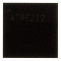
AT86RF212-ZU Atmel, AT86RF212-ZU Datasheet - Page 19

AT86RF212-ZU
Manufacturer Part Number
AT86RF212-ZU
Description
IC TXRX ZIGBE/802.15.4/ISM 32QFN
Manufacturer
Atmel
Datasheet
1.AT86RF212-ZU.pdf
(172 pages)
Specifications of AT86RF212-ZU
Frequency
700MHz, 800MHz, 900MHz
Data Rate - Maximum
250kbps
Modulation Or Protocol
802.15.4 Zigbee, 6LoWPAN, ISM
Applications
ISM, ZigBee™
Power - Output
10dBm
Sensitivity
-110dBm
Voltage - Supply
1.8 V ~ 3.6 V
Current - Receiving
9.2mA
Current - Transmitting
25mA
Data Interface
PCB, Surface Mount
Antenna Connector
PCB, Surface Mount
Operating Temperature
-40°C ~ 85°C
Package / Case
32-VQFN Exposed Pad, 32-HVQFN, 32-SQFN, 32-DHVQFN
Number Of Receivers
1
Number Of Transmitters
1
Wireless Frequency
769 MHz to 935 MHz
Interface Type
SPI
Noise Figure
7 dB
Output Power
21 dB
Operating Supply Voltage
1.8 V, 3 V
Maximum Operating Temperature
+ 85 C
Mounting Style
SMD/SMT
Maximum Supply Current
25 mA
Minimum Operating Temperature
- 40 C
Modulation
OQPSK
Protocol Supported
802.15.4
Operating Temperature (min)
-40C
Operating Temperature (max)
85C
Operating Temperature Classification
Industrial
Lead Free Status / RoHS Status
Lead free / RoHS Compliant
Memory Size
-
Lead Free Status / Rohs Status
Lead free / RoHS Compliant
Available stocks
Company
Part Number
Manufacturer
Quantity
Price
Company:
Part Number:
AT86RF212-ZU
Manufacturer:
HITTITE
Quantity:
5 000
Part Number:
AT86RF212-ZU
Manufacturer:
ATMEL/爱特梅尔
Quantity:
20 000
Part Number:
AT86RF212-ZUR
Manufacturer:
MICROCHIP/微芯
Quantity:
20 000
Figure 4-10. Exemplary SPI Sequence - Frame Buffer Write of a Frame with 4-byte PSDU
4.3.3 SRAM Access Mode
Figure 4-11. Packet Structure – SRAM Read Access
8168C-MCU Wireless-02/10
Access violations during a Frame Buffer read or write access are indicated by interrupt
IRQ_6 (TRX_UR). For further details, refer to section 7.4.
Notes
• The Frame Buffer is shared between RX and TX; therefore, the frame data are
• To avoid overwriting during receive, Dynamic Frame Buffer Protection can be
• For exceptions, e.g. receiving acknowledgement frames in Extended Operating Mode
The SRAM access mode allows accessing dedicated bytes within the Frame Buffer.
This may reduce the SPI traffic.
During frame receive, after occurrence of IRQ_2 (RX_START), a SRAM access can be
used to upload the PHR field while preserving Dynamic Frame Buffer Protection, see
section 9.7.
Each SRAM access starts with /SEL = L. The first transferred byte on MOSI shall be the
command byte and must indicate an SRAM access mode according to the definition in
Table 4-2. The following byte indicates the start address of the write or read access.
The address space is 0x00 to 0x7F for radio transceiver receive or transmit operations.
The security module (AES) uses an address space from 0x82 to 0x94; refer to
section 9.1.
On SRAM read access, one or more bytes of read data are transferred on MISO
starting with the third byte of the access sequence; refer to Figure 4-11.
On SRAM write access, one or more bytes of write data are transferred on MOSI
starting with the third byte of the access sequence; refer to Figure 4-12. Do not attempt
to read or write bytes beyond the SRAM buffer size.
overwritten by new incoming frames. If the TX frame data are to be retransmitted, it
must be ensured that no frame was received in the meanwhile.
enabled; refer to section 9.7.
(TX_ARET), refer to section 5.2.4.
AT86RF212
19


