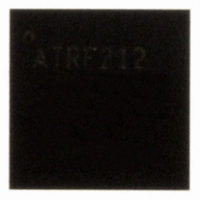
AT86RF212-ZU Atmel, AT86RF212-ZU Datasheet - Page 7

AT86RF212-ZU
Manufacturer Part Number
AT86RF212-ZU
Description
IC TXRX ZIGBE/802.15.4/ISM 32QFN
Manufacturer
Atmel
Datasheet
1.AT86RF212-ZU.pdf
(172 pages)
Specifications of AT86RF212-ZU
Frequency
700MHz, 800MHz, 900MHz
Data Rate - Maximum
250kbps
Modulation Or Protocol
802.15.4 Zigbee, 6LoWPAN, ISM
Applications
ISM, ZigBee™
Power - Output
10dBm
Sensitivity
-110dBm
Voltage - Supply
1.8 V ~ 3.6 V
Current - Receiving
9.2mA
Current - Transmitting
25mA
Data Interface
PCB, Surface Mount
Antenna Connector
PCB, Surface Mount
Operating Temperature
-40°C ~ 85°C
Package / Case
32-VQFN Exposed Pad, 32-HVQFN, 32-SQFN, 32-DHVQFN
Number Of Receivers
1
Number Of Transmitters
1
Wireless Frequency
769 MHz to 935 MHz
Interface Type
SPI
Noise Figure
7 dB
Output Power
21 dB
Operating Supply Voltage
1.8 V, 3 V
Maximum Operating Temperature
+ 85 C
Mounting Style
SMD/SMT
Maximum Supply Current
25 mA
Minimum Operating Temperature
- 40 C
Modulation
OQPSK
Protocol Supported
802.15.4
Operating Temperature (min)
-40C
Operating Temperature (max)
85C
Operating Temperature Classification
Industrial
Lead Free Status / RoHS Status
Lead free / RoHS Compliant
Memory Size
-
Lead Free Status / Rohs Status
Lead free / RoHS Compliant
Available stocks
Company
Part Number
Manufacturer
Quantity
Price
Company:
Part Number:
AT86RF212-ZU
Manufacturer:
HITTITE
Quantity:
5 000
Part Number:
AT86RF212-ZU
Manufacturer:
ATMEL/爱特梅尔
Quantity:
20 000
Part Number:
AT86RF212-ZUR
Manufacturer:
MICROCHIP/微芯
Quantity:
20 000
2.2.1.3 Crystal Oscillator Pins
2.2.1.4 Analog Pin Summary
Table 2-2. Analog Pin Behavior – DC Values
2.2.2 Digital Pins
2.2.2.1 Driver Strength Settings
Table 2-3. Digital Output Driver Configuration
8168C-MCU Wireless-02/10
Pin
RFP/RFN
XTAL1/XTAL2
DVDD
AVDD
Pin
MISO, IRQ, DIG1, … , DIG4
CLKM
Values and Conditions
V
V
V
V
C
V
V
V
SLEEP, RESET, and TRX_OFF)
V
DC
DC
DC
DC
DC
DC
DC
DC
PAR
= 0.9 V (BUSY_TX)
= 20 mV (receive states)
= 0 mV (otherwise)
= 0.9 V at both pins
= 1.8 V (all states, except SLEEP)
= 0 mV (otherwise)
= 1.8 V (all states, except P_ON,
= 0 mV (otherwise)
= 3 pF
XTAL1, XTAL2
The pin XTAL1 is the input of the reference oscillator amplifier (XOSC), XTAL2 the
output. A detailed description of the crystal oscillator setup and the related
XTAL1/XTAL2 pin configuration can be found in section 7.7.
When using an external clock reference signal, XTAL1 shall be used as input pin. For
further details, refer to section 7.7.3.
The AT86RF212 provides a digital microcontroller interface. The interface comprises a
slave SPI (/SEL, SCLK, MOSI, and MISO) and additional control signals (CLKM, IRQ,
SLP_TR, /RST, and DIG2). The microcontroller interface is described in detail in section
4.
Additional digital output signals DIG1 … DIG4 are provided to control external blocks,
i.e. for Antenna Diversity RF switch control or as an RX/TX Indicator; see sections 9.3
and 9.4 respectively. After reset, these pins are connected to digital ground
(DIG1/DIG2) or analog ground (DIG3/DIG4).
The driver strength of all digital output pins (MISO, IRQ, DIG1, … , DIG4) and CLKM
pin can be configured using register 0x03 (TRX_CTRL_0); see Table 2-3.
The capacitive load should be as small as possible and not larger than 50 pF when
using the 2 mA minimum driver strength setting. Generally, the output driver strength
should be adjusted to the lowest possible value in order to keep the current
consumption and the emission of digital signal harmonics low.
Default Driver Strength
2 mA
4 mA
Comments
DC level at pins RFP/RFN for various transceiver states
AC-coupling is required if an antenna with a DC path to ground is used.
Serial capacitance and capacitance of each pin to ground must be
< 100 pF.
DC level at pins XTAL1/XTAL2 for various transceiver states
Parasitic capacitance (C
load capacitance to the crystal.
DC level at pin DVDD for various transceiver states
Supply pins (voltage regulator output) for the digital 1.8 V voltage domain.
The outputs shall be bypassed by 1 µF.
DC level at pin AVDD for various transceiver states
Supply pin (voltage regulator output) for the analog 1.8 V voltage domain.
The outputs shall be bypassed by 1 µF.
Comment
Adjustable to 2 mA, 4 mA, 6 mA, and 8 mA
Adjustable to 2 mA, 4 mA, 6 mA, and 8 mA
PAR
) of the pins must be considered as additional
AT86RF212
7


