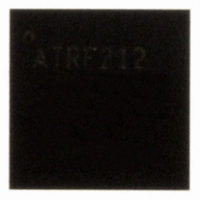
AT86RF212-ZU Atmel, AT86RF212-ZU Datasheet - Page 15

AT86RF212-ZU
Manufacturer Part Number
AT86RF212-ZU
Description
IC TXRX ZIGBE/802.15.4/ISM 32QFN
Manufacturer
Atmel
Datasheet
1.AT86RF212-ZU.pdf
(172 pages)
Specifications of AT86RF212-ZU
Frequency
700MHz, 800MHz, 900MHz
Data Rate - Maximum
250kbps
Modulation Or Protocol
802.15.4 Zigbee, 6LoWPAN, ISM
Applications
ISM, ZigBee™
Power - Output
10dBm
Sensitivity
-110dBm
Voltage - Supply
1.8 V ~ 3.6 V
Current - Receiving
9.2mA
Current - Transmitting
25mA
Data Interface
PCB, Surface Mount
Antenna Connector
PCB, Surface Mount
Operating Temperature
-40°C ~ 85°C
Package / Case
32-VQFN Exposed Pad, 32-HVQFN, 32-SQFN, 32-DHVQFN
Number Of Receivers
1
Number Of Transmitters
1
Wireless Frequency
769 MHz to 935 MHz
Interface Type
SPI
Noise Figure
7 dB
Output Power
21 dB
Operating Supply Voltage
1.8 V, 3 V
Maximum Operating Temperature
+ 85 C
Mounting Style
SMD/SMT
Maximum Supply Current
25 mA
Minimum Operating Temperature
- 40 C
Modulation
OQPSK
Protocol Supported
802.15.4
Operating Temperature (min)
-40C
Operating Temperature (max)
85C
Operating Temperature Classification
Industrial
Lead Free Status / RoHS Status
Lead free / RoHS Compliant
Memory Size
-
Lead Free Status / Rohs Status
Lead free / RoHS Compliant
Available stocks
Company
Part Number
Manufacturer
Quantity
Price
Company:
Part Number:
AT86RF212-ZU
Manufacturer:
HITTITE
Quantity:
5 000
Part Number:
AT86RF212-ZU
Manufacturer:
ATMEL/爱特梅尔
Quantity:
20 000
Part Number:
AT86RF212-ZUR
Manufacturer:
MICROCHIP/微芯
Quantity:
20 000
4.2 SPI Timing Description
Figure 4-2. SPI Timing: Global Map and Definition of Timing Parameters t
Figure 4-3. SPI Timing: Detailed Drawing of Timing Parameter t
8168C-MCU Wireless-02/10
Pin 17 (CLKM) can be used as a microcontroller master clock source. If the
microcontroller derives the SPI master clock (SCLK) directly from CLKM, the SPI
operates in synchronous mode, otherwise in asynchronous mode.
In synchronous mode, the maximum SCLK frequency is 8 MHz.
In asynchronous mode, the maximum SCLK frequency is limited to 7.5 MHz. The signal
at pin CLKM is not required to derive SCLK and may be disabled to reduce power
consumption and spurious emissions.
Figure 4-2 and Figure 4-3 illustrate the SPI timing and introduces its parameters. The
corresponding timing parameter definitions t
The SPI is based on a byte-oriented protocol and is always a bidirectional
communication between master and slave. The SPI master starts the transfer by
asserting /SEL = L. Then the master generates eight SPI clock cycles to transfer one
byte to the radio transceiver (via MOSI). At the same time, the slave transmits one byte
to the master (via MISO). When the master wants to receive one byte of data from the
slave, it must also transmit one byte to the slave. All bytes are transferred with MSB
first. An SPI transaction is finished by releasing /SEL = H.
/SEL = L enables the MISO output driver of the AT86RF212. The MSB of MISO is valid
after t
SCLK. If the driver is disabled, there is no internal pull-up resistor connected to it.
Driving the appropriate signal level must be ensured by the master device or an
external pull-up resistor. Note, when both /SEL and /RST are active, the MISO output
driver is also enabled.
1
(see section 10.4, parameter 10.4.3) and is updated at each falling edge of
1
, t
2
, t
3
, and t
5
, t
6
4
, t
1
– t
8
, and t
9
are defined in section 10.4.
9
AT86RF212
15


