PIC18C801-I/L Microchip Technology, PIC18C801-I/L Datasheet - Page 223
PIC18C801-I/L
Manufacturer Part Number
PIC18C801-I/L
Description
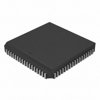
IC,MICROCONTROLLER,8-BIT,PIC CPU,CMOS,LDCC,84PIN,PLASTIC
Manufacturer
Microchip Technology
Series
PIC® 18Cr
Datasheets
1.PIC16F616T-ISL.pdf
(8 pages)
2.PIC18C601-IL.pdf
(320 pages)
3.PIC18C601-IL.pdf
(10 pages)
4.PIC18C601-IL.pdf
(10 pages)
Specifications of PIC18C801-I/L
Rohs Compliant
YES
Core Processor
PIC
Core Size
8-Bit
Speed
25MHz
Connectivity
EBI/EMI, I²C, SPI, UART/USART
Peripherals
Brown-out Detect/Reset, LVD, POR, PWM, WDT
Number Of I /o
37
Program Memory Type
ROMless
Ram Size
1.5K x 8
Voltage - Supply (vcc/vdd)
4.2 V ~ 5.5 V
Data Converters
A/D 12x10b
Oscillator Type
External
Operating Temperature
-40°C ~ 85°C
Package / Case
84-PLCC
Processor Series
PIC18C
Core
PIC
Data Bus Width
8 bit
Data Ram Size
1.5 KB
Interface Type
3-Wire, I2C, SPI, USART
Maximum Clock Frequency
25 MHz
Number Of Programmable I/os
47
Number Of Timers
1 x 16 bit
Operating Supply Voltage
2 V to 5.5 V
Maximum Operating Temperature
+ 85 C
Mounting Style
SMD/SMT
3rd Party Development Tools
52715-96, 52716-328, 52717-734, 52712-325, EWPIC18
Development Tools By Supplier
DV164005, ICE4000, DV164136
Minimum Operating Temperature
- 40 C
On-chip Adc
10 bit
Lead Free Status / RoHS Status
Lead free / RoHS Compliant
For Use With
AC164310 - MODULE SKT FOR PM3 84PLCCXLT84L1 - SOCKET TRANSITION ICE 84PLCCAC174012 - MODULE SKT PROMATEII 84PLCC
Eeprom Size
-
Program Memory Size
-
Lead Free Status / Rohs Status
Details
Other names
PIC18C801-I/LR
PIC18C801-I/LR
PIC18C801I/L
PIC18C801-I/LR
PIC18C801I/L
Available stocks
Company
Part Number
Manufacturer
Quantity
Price
Company:

Part Number:
PIC18C801-I/L
Manufacturer:
MICROCHIP
Quantity:
12 000
Company:
Part Number:
PIC18C801-I/L
Manufacturer:
Microchip Technology
Quantity:
10 000


ANDWF
Syntax:
Operands:
Operation:
Status Affected:
Encoding:
Description:
Words:
Cycles:
Q Cycle Activity:
Example:
2001 Microchip Technology Inc.
Before Instruction
After Instruction
Decode
WREG
REG
N
Z
WREG
REG
N
Z
Q1
=
=
=
=
=
=
=
=
register ’f’
AND WREG with f
[ label ] ANDWF
0
d
a
(WREG) .AND. (f)
N,Z
The contents of WREG are AND’ed
with register 'f'. If 'd' is 0, the result is
stored in WREG. If 'd' is 1, the result
is stored back in register 'f' (default).
If ’a’ is 0, the Access Bank will be
selected. If ’a’ is 1, the bank will be
selected as per the BSR value.
1
1
ANDWF
Read
0001
Q2
17h
0C2h
?
?
02h
0C2h
0
0
f
[0,1]
[0,1]
255
01da
REG, W
Process
Data
Q3
ffff
f [,d [,a]]
dest
destination
Advance Information
Write to
Q4
ffff
BC
Syntax:
Operands:
Operation:
Status Affected:
Encoding:
Description:
Words:
Cycles:
Q Cycle Activity:
If Jump:
Example:
If No Jump:
Before Instruction
After Instruction
Q1
operation
Decode
Decode
PC
If Carry
If Carry
No
Q1
PC
PC
PIC18C601/801
Read literal
Q2
Read literal
operation
Branch if Carry
[ label ] BC
-128
if carry bit is ’1’
None
If the Carry bit is ’1’, then the pro-
gram will branch.
The 2’s complement number ’2n’ is
added to the PC. Since the PC will
have incremented to fetch the next
instruction, the new address will be
PC+2+2n. This instruction is then a
two-cycle instruction.
1
1(2)
HERE
(PC) + 2 + 2n
1110
No
Q2
’n’
’n’
=
=
=
=
n
address (HERE)
1;
address (HERE+12)
0;
address (HERE+2)
127
0010
Q3
operation
BC
Process
Process
Data
Data
n
No
Q3
DS39541A-page 223
5
PC
nnnn
Write to PC
Q4
operation
operation
No
No
Q4
nnnn
Related parts for PIC18C801-I/L
Image
Part Number
Description
Manufacturer
Datasheet
Request
R

Part Number:
Description:
IC, 8BIT MCU, PIC18F, 40MHZ, LCC-44
Manufacturer:
Microchip Technology
Datasheet:
Part Number:
Description:
IC, 8BIT MCU, PIC18LF, 40MHZ, PLCC-64
Manufacturer:
Microchip Technology
Datasheet:
Part Number:
Description:
IC, 8BIT MCU, PIC18F, 64MHZ, TQFP-80
Manufacturer:
Microchip Technology
Datasheet:

Part Number:
Description:
MCU, MPU & DSP Development Tools CAN/LIN PICtail Plus Daughter Board
Manufacturer:
Microchip Technology
Datasheet:

Part Number:
Description:
IC, 8BIT MCU, PIC18F, 64MHZ, DIP-40
Manufacturer:
Microchip Technology
Datasheet:

Part Number:
Description:
IC, 8BIT MCU, PIC18LF, 40MHZ, PLCC-64
Manufacturer:
Microchip Technology
Datasheet:
Part Number:
Description:
IC, 8BIT MCU, PIC18F, 64MHZ, TQFP-64
Manufacturer:
Microchip Technology
Part Number:
Description:
IC, 8BIT MCU, PIC18F, 64MHZ, TQFP-80
Manufacturer:
Microchip Technology

Part Number:
Description:
8KB, Flash, 768bytes-RAM, 36I/O, 8-bit Family,nanowatt XLP 40 UQFN 5x5x0.5mm TUB
Manufacturer:
Microchip Technology
Datasheet:
Part Number:
Description:
8KB, Flash, 768bytes-RAM, 36I/O, 8-bit Family,nanowatt XLP 40 UQFN 5x5x0.5mm TUB
Manufacturer:
Microchip Technology
Part Number:
Description:
16KB, Flash, 768bytes-RAM, 36I/O, 8-bit Family,nanowatt XLP 40 UQFN 5x5x0.5mm TU
Manufacturer:
Microchip Technology
Datasheet:
Part Number:
Description:
16KB, Flash, 768bytes-RAM, 36I/O, 8-bit Family,nanowatt XLP 40 UQFN 5x5x0.5mm TU
Manufacturer:
Microchip Technology
Part Number:
Description:
32KB, Flash, 1536bytes-RAM, 36I/O, 8-bit Family,nanowatt XLP 40 UQFN 5x5x0.5mm T
Manufacturer:
Microchip Technology
Datasheet:
Part Number:
Description:
32KB, Flash, 1536bytes-RAM, 36I/O, 8-bit Family,nanowatt XLP 40 UQFN 5x5x0.5mm T
Manufacturer:
Microchip Technology
Part Number:
Description:
64KB, Flash, 3968bytes-RAM, 36I/O, 8-bit Family,nanowatt XLP 40 UQFN 5x5x0.5mm T
Manufacturer:
Microchip Technology
Datasheet: