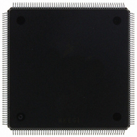
MCF5407AI220 Freescale Semiconductor, MCF5407AI220 Datasheet - Page 180

MCF5407AI220
Manufacturer Part Number
MCF5407AI220
Description
IC MPU 32B 220MHZ COLDF 208-FQFP
Manufacturer
Freescale Semiconductor
Series
MCF540xr
Specifications of MCF5407AI220
Core Processor
Coldfire V4
Core Size
32-Bit
Speed
220MHz
Connectivity
EBI/EMI, I²C, UART/USART
Peripherals
DMA, WDT
Number Of I /o
16
Program Memory Type
ROMless
Ram Size
4K x 8
Voltage - Supply (vcc/vdd)
1.65 V ~ 3.6 V
Oscillator Type
External
Operating Temperature
0°C ~ 70°C
Package / Case
208-FQFP
Maximum Clock Frequency
220 MHz
Operating Supply Voltage
1.8 V, 3.3 V
Maximum Operating Temperature
+ 105 C
Mounting Style
SMD/SMT
Minimum Operating Temperature
0 C
Program Memory Size
24KB
Cpu Speed
220MHz
Embedded Interface Type
I2C, UART
Digital Ic Case Style
FQFP
No. Of Pins
208
Supply Voltage Range
3.3V
Rohs Compliant
Yes
For Use With
M5407C3 - KIT EVAL FOR MCF5407 W/ETHERNET
Lead Free Status / RoHS Status
Lead free / RoHS Compliant
Eeprom Size
-
Program Memory Size
-
Data Converters
-
Lead Free Status / Rohs Status
Lead free / RoHS Compliant
Available stocks
Company
Part Number
Manufacturer
Quantity
Price
Company:
Part Number:
MCF5407AI220
Manufacturer:
freescaie
Quantity:
6
Company:
Part Number:
MCF5407AI220
Manufacturer:
Freescale Semiconductor
Quantity:
135
Company:
Part Number:
MCF5407AI220
Manufacturer:
FREESCALE
Quantity:
1 831
Company:
Part Number:
MCF5407AI220
Manufacturer:
Freescale Semiconductor
Quantity:
10 000
- Current page: 180 of 546
- Download datasheet (7Mb)
Background Debug Mode (BDM)
Thus, a count of either nine or more sequential single 0xF values or five or more sequential
0xFF values signifies the HALT condition.
5.5.2 BDM Serial Interface
When the CPU is halted and PSTDDATA reflects the halt status, the development system
can send unrestricted commands to the debug module. The debug module implements a
synchronous protocol using two inputs (DSCLK and DSI) and one output (DSO), where
DSCLK and DSI must meet the required input setup and hold timings and the DSO is
specified as a delay relative to the rising edge of the processor clock. See Table 5-1. The
development system serves as the serial communication channel master and must generate
DSCLK.
The serial channel operates at a frequency from DC to 1/5 of the processor frequency. The
channel uses full-duplex mode, where data is sent and received simultaneously by both
master and slave devices. The transmission consists of 17-bit packets composed of a
status/control bit and a 16-bit data word. As shown in Figure 5-15, all state transitions are
enabled on a rising edge of the processor clock when DSCLK is high; that is, DSI is
sampled and DSO is driven.
5-24
• A B marker occurs on the right nibble of PSTDDATA with the data of 0xFF
BDM State
CPU CLK
following:
PSTDDATA[7:0]
0xYB
0xFF
0xFF
0xFF
0xFF
0xXY (X indicates that the PST value is guaranteed to not be 0xF; and Y indicates
a PSTDDATA value that doesn’t affect the 0xFF count).
PSTCLK
Machine
DSCLK
DSO
DSI
Figure 5-15. BDM Serial Interface Timing
Current State
Past
C1
MCF5407 User’s Manual
Current
C2
C3
C4
Next State
Current
Next
Related parts for MCF5407AI220
Image
Part Number
Description
Manufacturer
Datasheet
Request
R
Part Number:
Description:
Mcf5407 Coldfire Integrated Microprocessor User
Manufacturer:
Freescale Semiconductor, Inc
Datasheet:
Part Number:
Description:
Manufacturer:
Freescale Semiconductor, Inc
Datasheet:
Part Number:
Description:
Manufacturer:
Freescale Semiconductor, Inc
Datasheet:
Part Number:
Description:
Manufacturer:
Freescale Semiconductor, Inc
Datasheet:
Part Number:
Description:
Manufacturer:
Freescale Semiconductor, Inc
Datasheet:
Part Number:
Description:
Manufacturer:
Freescale Semiconductor, Inc
Datasheet:
Part Number:
Description:
Manufacturer:
Freescale Semiconductor, Inc
Datasheet:
Part Number:
Description:
Manufacturer:
Freescale Semiconductor, Inc
Datasheet:
Part Number:
Description:
Manufacturer:
Freescale Semiconductor, Inc
Datasheet:
Part Number:
Description:
Manufacturer:
Freescale Semiconductor, Inc
Datasheet:
Part Number:
Description:
Manufacturer:
Freescale Semiconductor, Inc
Datasheet:
Part Number:
Description:
Manufacturer:
Freescale Semiconductor, Inc
Datasheet:
Part Number:
Description:
Manufacturer:
Freescale Semiconductor, Inc
Datasheet:
Part Number:
Description:
Manufacturer:
Freescale Semiconductor, Inc
Datasheet:
Part Number:
Description:
Manufacturer:
Freescale Semiconductor, Inc
Datasheet:


