MCF5407AI220 Freescale Semiconductor, MCF5407AI220 Datasheet - Page 27
MCF5407AI220
Manufacturer Part Number
MCF5407AI220
Description
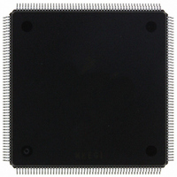
IC MPU 32B 220MHZ COLDF 208-FQFP
Manufacturer
Freescale Semiconductor
Series
MCF540xr
Specifications of MCF5407AI220
Core Processor
Coldfire V4
Core Size
32-Bit
Speed
220MHz
Connectivity
EBI/EMI, I²C, UART/USART
Peripherals
DMA, WDT
Number Of I /o
16
Program Memory Type
ROMless
Ram Size
4K x 8
Voltage - Supply (vcc/vdd)
1.65 V ~ 3.6 V
Oscillator Type
External
Operating Temperature
0°C ~ 70°C
Package / Case
208-FQFP
Maximum Clock Frequency
220 MHz
Operating Supply Voltage
1.8 V, 3.3 V
Maximum Operating Temperature
+ 105 C
Mounting Style
SMD/SMT
Minimum Operating Temperature
0 C
Program Memory Size
24KB
Cpu Speed
220MHz
Embedded Interface Type
I2C, UART
Digital Ic Case Style
FQFP
No. Of Pins
208
Supply Voltage Range
3.3V
Rohs Compliant
Yes
For Use With
M5407C3 - KIT EVAL FOR MCF5407 W/ETHERNET
Lead Free Status / RoHS Status
Lead free / RoHS Compliant
Eeprom Size
-
Program Memory Size
-
Data Converters
-
Lead Free Status / Rohs Status
Lead free / RoHS Compliant
Available stocks
Company
Part Number
Manufacturer
Quantity
Price
Company:

Part Number:
MCF5407AI220
Manufacturer:
freescaie
Quantity:
6
Company:
Part Number:
MCF5407AI220
Manufacturer:
Freescale Semiconductor
Quantity:
135
Company:
Part Number:
MCF5407AI220
Manufacturer:
FREESCALE
Quantity:
1 831
Company:
Part Number:
MCF5407AI220
Manufacturer:
Freescale Semiconductor
Quantity:
10 000


Figure
Number
20-5
20-6
20-7
20-8
20-9
20-10
20-11
20-12
20-13
20-14
20-15
20-16
20-17
20-18
20-19
20-20
20-21
20-22
20-23
20-24
A-1
A-2
A-3
A-4
A-5
A-6
A-7
PSTCLK Timing......................................................................................................... 20-6
AC Timings—Normal Read and Write Bus Cycles ................................................... 20-8
SDRAM Read Cycle with EDGESEL Tied to Buffered CLKIN ............................... 20-9
SDRAM Write Cycle with EDGESEL Tied to Buffered CLKIN ............................ 20-10
SDRAM Read Cycle with EDGESEL Tied High..................................................... 20-11
SDRAM Write Cycle with EDGESEL Tied High.................................................... 20-12
SDRAM Read Cycle with EDGESEL Tied Low ..................................................... 20-13
SDRAM Write Cycle with EDGESEL Tied Low .................................................... 20-14
AC Output Timing—High Impedance...................................................................... 20-14
Reset Timing............................................................................................................. 20-15
Real-Time Trace AC Timing .................................................................................... 20-16
BDM Serial Port AC Timing .................................................................................... 20-16
Timer Module AC Timing ........................................................................................ 20-17
I
UART0 and UART1 Module AC Timing—UART Mode ....................................... 20-20
UART1 in 8- and 16-bit CODEC Mode ................................................................... 20-21
UART1 in AC ‘97 Mode .......................................................................................... 20-21
General-Purpose I/O Timing..................................................................................... 20-22
DMA Timing ............................................................................................................ 20-23
IEEE 1149.1 (JTAG) AC Timing ............................................................................. 20-25
MCF5307 to MCF5407 TM[2:0] Pin Remapping ....................................................... A-5
Simplified Block Diagram ........................................................................................... A-6
PLL Module................................................................................................................. A-7
Exception Stack Frame Form .................................................................................... A-11
Write Debug Module Register Command (
WDMREG
PLL Power Supply Filter Circuit............................................................................... A-18
2
C Input/Output Timings ......................................................................................... 20-19
Command Sequence................................................................................... A-13
ILLUSTRATIONS
Illustrations
Title
WDMREG
)............................................... A-12
Number
Page
xxvii
Related parts for MCF5407AI220
Image
Part Number
Description
Manufacturer
Datasheet
Request
R

Part Number:
Description:
Mcf5407 Coldfire Integrated Microprocessor User
Manufacturer:
Freescale Semiconductor, Inc
Datasheet:
Part Number:
Description:
Manufacturer:
Freescale Semiconductor, Inc
Datasheet:
Part Number:
Description:
Manufacturer:
Freescale Semiconductor, Inc
Datasheet:
Part Number:
Description:
Manufacturer:
Freescale Semiconductor, Inc
Datasheet:
Part Number:
Description:
Manufacturer:
Freescale Semiconductor, Inc
Datasheet:
Part Number:
Description:
Manufacturer:
Freescale Semiconductor, Inc
Datasheet:
Part Number:
Description:
Manufacturer:
Freescale Semiconductor, Inc
Datasheet:
Part Number:
Description:
Manufacturer:
Freescale Semiconductor, Inc
Datasheet:
Part Number:
Description:
Manufacturer:
Freescale Semiconductor, Inc
Datasheet:
Part Number:
Description:
Manufacturer:
Freescale Semiconductor, Inc
Datasheet:
Part Number:
Description:
Manufacturer:
Freescale Semiconductor, Inc
Datasheet:
Part Number:
Description:
Manufacturer:
Freescale Semiconductor, Inc
Datasheet:
Part Number:
Description:
Manufacturer:
Freescale Semiconductor, Inc
Datasheet:
Part Number:
Description:
Manufacturer:
Freescale Semiconductor, Inc
Datasheet:
Part Number:
Description:
Manufacturer:
Freescale Semiconductor, Inc
Datasheet: