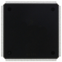
MCF5407AI220 Freescale Semiconductor, MCF5407AI220 Datasheet - Page 272

MCF5407AI220
Manufacturer Part Number
MCF5407AI220
Description
IC MPU 32B 220MHZ COLDF 208-FQFP
Manufacturer
Freescale Semiconductor
Series
MCF540xr
Specifications of MCF5407AI220
Core Processor
Coldfire V4
Core Size
32-Bit
Speed
220MHz
Connectivity
EBI/EMI, I²C, UART/USART
Peripherals
DMA, WDT
Number Of I /o
16
Program Memory Type
ROMless
Ram Size
4K x 8
Voltage - Supply (vcc/vdd)
1.65 V ~ 3.6 V
Oscillator Type
External
Operating Temperature
0°C ~ 70°C
Package / Case
208-FQFP
Maximum Clock Frequency
220 MHz
Operating Supply Voltage
1.8 V, 3.3 V
Maximum Operating Temperature
+ 105 C
Mounting Style
SMD/SMT
Minimum Operating Temperature
0 C
Program Memory Size
24KB
Cpu Speed
220MHz
Embedded Interface Type
I2C, UART
Digital Ic Case Style
FQFP
No. Of Pins
208
Supply Voltage Range
3.3V
Rohs Compliant
Yes
For Use With
M5407C3 - KIT EVAL FOR MCF5407 W/ETHERNET
Lead Free Status / RoHS Status
Lead free / RoHS Compliant
Eeprom Size
-
Program Memory Size
-
Data Converters
-
Lead Free Status / Rohs Status
Lead free / RoHS Compliant
Available stocks
Company
Part Number
Manufacturer
Quantity
Price
Company:
Part Number:
MCF5407AI220
Manufacturer:
freescaie
Quantity:
6
Company:
Part Number:
MCF5407AI220
Manufacturer:
Freescale Semiconductor
Quantity:
135
Company:
Part Number:
MCF5407AI220
Manufacturer:
FREESCALE
Quantity:
1 831
Company:
Part Number:
MCF5407AI220
Manufacturer:
Freescale Semiconductor
Quantity:
10 000
- Current page: 272 of 546
- Download datasheet (7Mb)
Asynchronous Operation
11.3 Asynchronous Operation
The DRAM controller supports asynchronous DRAMs for cost-effective systems. Typical
access times for the DRAM controller interfacing to ADRAM are 4-3-3-3. The DRAM
controller supports the following four asynchronous modes:
In asynchronous mode, RAS and CAS always transition at the falling clock edge. As
summarized previously, operation and timing of each ADRAM block is controlled by
separate registers, but refresh is the same for both. All ADRAM accesses should be
terminated by the DRAM controller. There is no priority encoding between memory
blocks, so programming blocks to overlap with other blocks or with other internal resources
causes undefined behavior.
11.3.1 DRAM Controller Signals in Asynchronous Mode
Table 11-2 summarizes DRAM signals used in asynchronous mode.
11.3.2 Asynchronous Register Set
The following register configurations apply when DCR[SO] is 0, indicating the DRAM
controller is interfacing to asynchronous DRAMs.
11.3.2.1 DRAM Control Register (DCR) in Asynchronous Mode
The DCR provides programmable options for the refresh logic as well as the control bit to
determine if the module is operating with synchronous or asynchronous DRAMs. The DCR
is shown in Figure 11-2.
RAS[1:0]
CAS[3:0]
DRAMW
11-4
Signal
• Non-page mode
• Burst page mode
• Continuous page mode
• Extended data-out mode
Row address strobes. Interface to RAS inputs on industry-standard ADRAMs. When SDRAMs are used,
these signals interface to the chip-select lines within an SDRAM’s memory block. Thus, there is one RAS
line for each of the two blocks.
Column address strobes. Interface to CAS inputs on industry-standard DRAMs. These provide CAS for
a given ADRAM block. When SDRAMs are used, CAS[3:0] control the byte enables (DQMx) for standard
SDRAMs. CAS[3:0] strobes data in least-to-most significant byte order (CAS0 is MSB).
DRAM read/write. Asserted when a DRAM write cycle is underway. Negated for read bus cycles.
Table 11-2. SDRAM Signal Summary
MCF5407 User’s Manual
Description
Related parts for MCF5407AI220
Image
Part Number
Description
Manufacturer
Datasheet
Request
R
Part Number:
Description:
Mcf5407 Coldfire Integrated Microprocessor User
Manufacturer:
Freescale Semiconductor, Inc
Datasheet:
Part Number:
Description:
Manufacturer:
Freescale Semiconductor, Inc
Datasheet:
Part Number:
Description:
Manufacturer:
Freescale Semiconductor, Inc
Datasheet:
Part Number:
Description:
Manufacturer:
Freescale Semiconductor, Inc
Datasheet:
Part Number:
Description:
Manufacturer:
Freescale Semiconductor, Inc
Datasheet:
Part Number:
Description:
Manufacturer:
Freescale Semiconductor, Inc
Datasheet:
Part Number:
Description:
Manufacturer:
Freescale Semiconductor, Inc
Datasheet:
Part Number:
Description:
Manufacturer:
Freescale Semiconductor, Inc
Datasheet:
Part Number:
Description:
Manufacturer:
Freescale Semiconductor, Inc
Datasheet:
Part Number:
Description:
Manufacturer:
Freescale Semiconductor, Inc
Datasheet:
Part Number:
Description:
Manufacturer:
Freescale Semiconductor, Inc
Datasheet:
Part Number:
Description:
Manufacturer:
Freescale Semiconductor, Inc
Datasheet:
Part Number:
Description:
Manufacturer:
Freescale Semiconductor, Inc
Datasheet:
Part Number:
Description:
Manufacturer:
Freescale Semiconductor, Inc
Datasheet:
Part Number:
Description:
Manufacturer:
Freescale Semiconductor, Inc
Datasheet:


