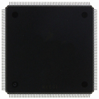
MCF5407AI220 Freescale Semiconductor, MCF5407AI220 Datasheet - Page 440

MCF5407AI220
Manufacturer Part Number
MCF5407AI220
Description
IC MPU 32B 220MHZ COLDF 208-FQFP
Manufacturer
Freescale Semiconductor
Series
MCF540xr
Specifications of MCF5407AI220
Core Processor
Coldfire V4
Core Size
32-Bit
Speed
220MHz
Connectivity
EBI/EMI, I²C, UART/USART
Peripherals
DMA, WDT
Number Of I /o
16
Program Memory Type
ROMless
Ram Size
4K x 8
Voltage - Supply (vcc/vdd)
1.65 V ~ 3.6 V
Oscillator Type
External
Operating Temperature
0°C ~ 70°C
Package / Case
208-FQFP
Maximum Clock Frequency
220 MHz
Operating Supply Voltage
1.8 V, 3.3 V
Maximum Operating Temperature
+ 105 C
Mounting Style
SMD/SMT
Minimum Operating Temperature
0 C
Program Memory Size
24KB
Cpu Speed
220MHz
Embedded Interface Type
I2C, UART
Digital Ic Case Style
FQFP
No. Of Pins
208
Supply Voltage Range
3.3V
Rohs Compliant
Yes
For Use With
M5407C3 - KIT EVAL FOR MCF5407 W/ETHERNET
Lead Free Status / RoHS Status
Lead free / RoHS Compliant
Eeprom Size
-
Program Memory Size
-
Data Converters
-
Lead Free Status / Rohs Status
Lead free / RoHS Compliant
Available stocks
Company
Part Number
Manufacturer
Quantity
Price
Company:
Part Number:
MCF5407AI220
Manufacturer:
freescaie
Quantity:
6
Company:
Part Number:
MCF5407AI220
Manufacturer:
Freescale Semiconductor
Quantity:
135
Company:
Part Number:
MCF5407AI220
Manufacturer:
FREESCALE
Quantity:
1 831
Company:
Part Number:
MCF5407AI220
Manufacturer:
Freescale Semiconductor
Quantity:
10 000
- Current page: 440 of 546
- Download datasheet (7Mb)
Data Transfer Operation
18.4.7.1 Line Transfers
A line is a 16-byte-aligned, 16-byte value. Despite the alignment, a line access may not
begin on the aligned address; therefore, the bus interface supports line transfers on multiple
address boundaries. Table 18-5 shows allowable patterns for line accesses.
18.4.7.2 Line Read Bus Cycles
Figure 18-12 shows line read with zero wait states. The access starts like a basic read bus
cycle with the first data transfer sampled on the rising edge of S4, but the next pipelined
burst data is sampled a cycle later on the rising edge of S6. Each subsequent pipelined data
burst is single cycle until the last one, which can be held for up to 2 CLKIN cycles after TA
is asserted. Note that AS and CSx are asserted throughout the burst transfer. This example
shows the timing for external termination, which differs only from the internal termination
example in Figure 18-13 in that the address lines change only at the beginning (assertion of
TS and TIP) and end (negation of TIP) of the transfer.
Figure 18-13 shows timing when internal termination is used.
18-12
TM[2:0], SIZ[1:0]
A[31:0], TT[1:0]
BE/BWEx, OE
AS, CSx
D[31:0]
CLKIN
R/W
TIP
TS
TA
Figure 18-12. Line Read Burst (2-1-1-1), External Termination
Table 18-5. Allowable Line Access Patterns
S0
A[3:2]
S1
00
01
10
11
S2
MCF5407 User’s Manual
S3
Read
S4
S5
Read
Longword Accesses
S6
0–4–8–C
4–8–C–0
8–C–0–4
C–0–4–8
Read
S7
S8
S9
Read
S10
S11 S12
Related parts for MCF5407AI220
Image
Part Number
Description
Manufacturer
Datasheet
Request
R
Part Number:
Description:
Mcf5407 Coldfire Integrated Microprocessor User
Manufacturer:
Freescale Semiconductor, Inc
Datasheet:
Part Number:
Description:
Manufacturer:
Freescale Semiconductor, Inc
Datasheet:
Part Number:
Description:
Manufacturer:
Freescale Semiconductor, Inc
Datasheet:
Part Number:
Description:
Manufacturer:
Freescale Semiconductor, Inc
Datasheet:
Part Number:
Description:
Manufacturer:
Freescale Semiconductor, Inc
Datasheet:
Part Number:
Description:
Manufacturer:
Freescale Semiconductor, Inc
Datasheet:
Part Number:
Description:
Manufacturer:
Freescale Semiconductor, Inc
Datasheet:
Part Number:
Description:
Manufacturer:
Freescale Semiconductor, Inc
Datasheet:
Part Number:
Description:
Manufacturer:
Freescale Semiconductor, Inc
Datasheet:
Part Number:
Description:
Manufacturer:
Freescale Semiconductor, Inc
Datasheet:
Part Number:
Description:
Manufacturer:
Freescale Semiconductor, Inc
Datasheet:
Part Number:
Description:
Manufacturer:
Freescale Semiconductor, Inc
Datasheet:
Part Number:
Description:
Manufacturer:
Freescale Semiconductor, Inc
Datasheet:
Part Number:
Description:
Manufacturer:
Freescale Semiconductor, Inc
Datasheet:
Part Number:
Description:
Manufacturer:
Freescale Semiconductor, Inc
Datasheet:


