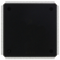
MCF5407AI220 Freescale Semiconductor, MCF5407AI220 Datasheet - Page 421

MCF5407AI220
Manufacturer Part Number
MCF5407AI220
Description
IC MPU 32B 220MHZ COLDF 208-FQFP
Manufacturer
Freescale Semiconductor
Series
MCF540xr
Specifications of MCF5407AI220
Core Processor
Coldfire V4
Core Size
32-Bit
Speed
220MHz
Connectivity
EBI/EMI, I²C, UART/USART
Peripherals
DMA, WDT
Number Of I /o
16
Program Memory Type
ROMless
Ram Size
4K x 8
Voltage - Supply (vcc/vdd)
1.65 V ~ 3.6 V
Oscillator Type
External
Operating Temperature
0°C ~ 70°C
Package / Case
208-FQFP
Maximum Clock Frequency
220 MHz
Operating Supply Voltage
1.8 V, 3.3 V
Maximum Operating Temperature
+ 105 C
Mounting Style
SMD/SMT
Minimum Operating Temperature
0 C
Program Memory Size
24KB
Cpu Speed
220MHz
Embedded Interface Type
I2C, UART
Digital Ic Case Style
FQFP
No. Of Pins
208
Supply Voltage Range
3.3V
Rohs Compliant
Yes
For Use With
M5407C3 - KIT EVAL FOR MCF5407 W/ETHERNET
Lead Free Status / RoHS Status
Lead free / RoHS Compliant
Eeprom Size
-
Program Memory Size
-
Data Converters
-
Lead Free Status / Rohs Status
Lead free / RoHS Compliant
Available stocks
Company
Part Number
Manufacturer
Quantity
Price
Company:
Part Number:
MCF5407AI220
Manufacturer:
freescaie
Quantity:
6
Company:
Part Number:
MCF5407AI220
Manufacturer:
Freescale Semiconductor
Quantity:
135
Company:
Part Number:
MCF5407AI220
Manufacturer:
FREESCALE
Quantity:
1 831
Company:
Part Number:
MCF5407AI220
Manufacturer:
Freescale Semiconductor
Quantity:
10 000
- Current page: 421 of 546
- Download datasheet (7Mb)
17.5.5.4 D3—Byte-Enable Configuration (BE_CONFIG)
The default byte-enable mode of the boot CS0 is determined by the logic level driven on
D3 at the rising edge of RSTI. This logic level is reflected as the reset value of
CSCR0[BEM]. Table 17-13 shows how the logic levels of D[6:5] correspond to the port
size for CS0 at reset.
17.5.6 D4—Address Configuration (ADDR_CONFIG)
The address configuration signal (ADDR_CONFIG) programs the PAR of the parallel I/O
port to be either parallel I/O or to be the upper address bus bits along with various attribute
and control signals at reset to give the user the option to access a broader addressing range
of memory if desired. ADDR_CONFIG is multiplexed with D4 and its configuration is
sampled at reset as shown in Table 17-15.
17.5.6.1 D[2:0]
The divide control input bus, DIVIDE[2:0], indicates the CLKIN/PCLK ratio. These
signals are sampled on the rising edge of RSTI to indicate the ratios described in
Chapter 20, “Electrical Specifications.”
17.6 Chip-Select Module Signals
The MCF5407 device provides eight programmable chip-select signals that can directly
interface with SRAM, EPROM, EEPROM, and peripherals. These signals are asserted and
negated on the falling edge of the clock.
17.6.1 Chip-Select (CS[7:0])
Each chip select can be programmed for a base address location and for masking addresses,
port size and burst-capability indication, wait-state generation, and internal/external
termination.
Reset clears all chip select programming; CS0 is the only chip select initialized out of reset.
CS0 is also unique because it can function at reset as a global chip select that allows boot
D3 (CSCR0[BEM])
D4/ADDR_CONFIG
0
1
Table 17-15. D4/ADDR_CONFIG, Address Pin Assignment
Table 17-14. D3/BE_CONFIG, BE[3:0] Boot Configuration
0
1
—
Neither BE nor BWE is asserted for read. BWE is generated for data write only.
BE is asserted for read; BWE is asserted for write.
Divide Control (DIVIDE[2:0])
PP[15:0], defaulted to inputs upon reset
A[31:24]/TIP/DREQ[1:0]/TM[2:0]/TT[1:0]
Chapter 17. Signal Descriptions
Boot CS0 Byte Enable Configuration
PAR Configuration at Reset
Chip-Select Module Signals
17-15
Related parts for MCF5407AI220
Image
Part Number
Description
Manufacturer
Datasheet
Request
R
Part Number:
Description:
Mcf5407 Coldfire Integrated Microprocessor User
Manufacturer:
Freescale Semiconductor, Inc
Datasheet:
Part Number:
Description:
Manufacturer:
Freescale Semiconductor, Inc
Datasheet:
Part Number:
Description:
Manufacturer:
Freescale Semiconductor, Inc
Datasheet:
Part Number:
Description:
Manufacturer:
Freescale Semiconductor, Inc
Datasheet:
Part Number:
Description:
Manufacturer:
Freescale Semiconductor, Inc
Datasheet:
Part Number:
Description:
Manufacturer:
Freescale Semiconductor, Inc
Datasheet:
Part Number:
Description:
Manufacturer:
Freescale Semiconductor, Inc
Datasheet:
Part Number:
Description:
Manufacturer:
Freescale Semiconductor, Inc
Datasheet:
Part Number:
Description:
Manufacturer:
Freescale Semiconductor, Inc
Datasheet:
Part Number:
Description:
Manufacturer:
Freescale Semiconductor, Inc
Datasheet:
Part Number:
Description:
Manufacturer:
Freescale Semiconductor, Inc
Datasheet:
Part Number:
Description:
Manufacturer:
Freescale Semiconductor, Inc
Datasheet:
Part Number:
Description:
Manufacturer:
Freescale Semiconductor, Inc
Datasheet:
Part Number:
Description:
Manufacturer:
Freescale Semiconductor, Inc
Datasheet:
Part Number:
Description:
Manufacturer:
Freescale Semiconductor, Inc
Datasheet:


