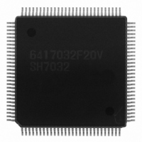
HD6417032F20V Renesas Electronics America, HD6417032F20V Datasheet - Page 184

HD6417032F20V
Manufacturer Part Number
HD6417032F20V
Description
SH1 ROMLESS LEAD FREE
Manufacturer
Renesas Electronics America
Series
SuperH® SH7030r
Datasheet
1.HD6417034AFI20.pdf
(689 pages)
Specifications of HD6417032F20V
Core Processor
SH-1
Core Size
32-Bit
Speed
20MHz
Connectivity
EBI/EMI, SCI
Peripherals
DMA, POR, PWM, WDT
Number Of I /o
32
Program Memory Type
ROMless
Ram Size
4K x 8
Voltage - Supply (vcc/vdd)
4.5 V ~ 5.5 V
Data Converters
A/D 8x10b
Oscillator Type
Internal
Operating Temperature
-20°C ~ 75°C
Package / Case
112-QFP
Lead Free Status / RoHS Status
Lead free / RoHS Compliant
Eeprom Size
-
Program Memory Size
-
Available stocks
Company
Part Number
Manufacturer
Quantity
Price
Company:
Part Number:
HD6417032F20V
Manufacturer:
TI
Quantity:
201
- Current page: 184 of 689
- Download datasheet (5Mb)
Section 8 Bus State Controller (BSC)
RAS Down Mode and RAS Up Mode: Sometimes access to another area can occur between
accesses to the DRAM even though burst operation has been selected. Keeping the RAS signal
low while this other access is occurring allows burst operation to continue the next time the same
row of the DRAM is accessed. The RASD bit in DCR selects RAS down mode when set to 1 and
RAS up mode when cleared to 0. In both RAS down mode and RAS up mode, burst operation is
continued while the same row address continues to be accessed, even if the bus master is changed.
Rev. 7.00 Jan 31, 2006 page 156 of 658
REJ09B0272-0700
The high-level duty of the CAS signal can be selected in short-pitch, high-speed page mode
using the CAS duty bit (CDTY) in DCR. When the CDTY bit is cleared to 0, the high-level
duty is 50% of the T
Long-pitch, high-speed page mode: When the RW1, WW1, DRW1, and DWW1 bits in WCR1
and WCR2 are set to 1, and the corresponding DRAM access cycle is continuing, the CAS
signal and column address output cycles (2 states) continue as long as the row addresses
continue to match. When the WAIT signal is detected at the low level, the second cycle of the
column address output cycle is repeated as the wait state. Figure 8.26 shows the timing for
long-pitch, high-speed page mode. See sections 20.1.3 (3) and 20.2.3 (3), Bus Timing, for
more information about the timing.
RAS down mode: When the RASD bit in DCR is set to 1, the DRAM access pauses and the
RAS signal is held low throughout the access of the other space while waiting for the next
Read
Write
AD15–AD0
AD15–AD0
Figure 8.26 Long-Pitch, High-Speed Page Mode (Read/Write Cycle)
A21–AD0
RAS
CAS
WR
WR
CK
C
state; when CDTY is set to 1, it is 35% of the T
Row address 1
T
p
T
r
Column address 1
T
c
1
Data 1
T
c
2
Data 1
Column address 2
T
c
1
C
state.
Data 2
T
c
2
Data 2
Related parts for HD6417032F20V
Image
Part Number
Description
Manufacturer
Datasheet
Request
R

Part Number:
Description:
KIT STARTER FOR M16C/29
Manufacturer:
Renesas Electronics America
Datasheet:

Part Number:
Description:
KIT STARTER FOR R8C/2D
Manufacturer:
Renesas Electronics America
Datasheet:

Part Number:
Description:
R0K33062P STARTER KIT
Manufacturer:
Renesas Electronics America
Datasheet:

Part Number:
Description:
KIT STARTER FOR R8C/23 E8A
Manufacturer:
Renesas Electronics America
Datasheet:

Part Number:
Description:
KIT STARTER FOR R8C/25
Manufacturer:
Renesas Electronics America
Datasheet:

Part Number:
Description:
KIT STARTER H8S2456 SHARPE DSPLY
Manufacturer:
Renesas Electronics America
Datasheet:

Part Number:
Description:
KIT STARTER FOR R8C38C
Manufacturer:
Renesas Electronics America
Datasheet:

Part Number:
Description:
KIT STARTER FOR R8C35C
Manufacturer:
Renesas Electronics America
Datasheet:

Part Number:
Description:
KIT STARTER FOR R8CL3AC+LCD APPS
Manufacturer:
Renesas Electronics America
Datasheet:

Part Number:
Description:
KIT STARTER FOR RX610
Manufacturer:
Renesas Electronics America
Datasheet:

Part Number:
Description:
KIT STARTER FOR R32C/118
Manufacturer:
Renesas Electronics America
Datasheet:

Part Number:
Description:
KIT DEV RSK-R8C/26-29
Manufacturer:
Renesas Electronics America
Datasheet:

Part Number:
Description:
KIT STARTER FOR SH7124
Manufacturer:
Renesas Electronics America
Datasheet:

Part Number:
Description:
KIT STARTER FOR H8SX/1622
Manufacturer:
Renesas Electronics America
Datasheet:

Part Number:
Description:
KIT DEV FOR SH7203
Manufacturer:
Renesas Electronics America
Datasheet:


