MCIMX53-START Freescale Semiconductor, MCIMX53-START Datasheet - Page 21
MCIMX53-START
Manufacturer Part Number
MCIMX53-START
Description
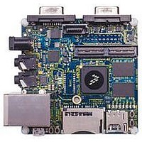
KIT DEVELOPMENT I.MX53
Manufacturer
Freescale Semiconductor
Series
i.MX53r
Type
MCUr
Datasheets
1.MCIMX53-START.pdf
(2 pages)
2.MCIMX53-START.pdf
(180 pages)
3.MCIMX53-START.pdf
(204 pages)
Specifications of MCIMX53-START
Contents
Board
Silicon Manufacturer
Freescale
Core Architecture
ARM
Core Sub-architecture
Cortex - A8
Silicon Core Number
I.MX5
Silicon Family Name
I.MX53
Peak Reflow Compatible (260 C)
Yes
Rohs Compliant
Yes
Leaded Process Compatible
Yes
Lead Free Status / RoHS Status
Lead free / RoHS Compliant
For Use With/related Products
i.MX53
Lead Free Status / Rohs Status
Supplier Unconfirmed
Available stocks
Company
Part Number
Manufacturer
Quantity
Price


4.1.4
The i.MX53xD device has four external input system clocks, a low frequency (CKIL), a high frequency
(XTAL), and two general purpose CKIH1 and CKIH2 clocks.
The CKIL is used for low-frequency functions. It supplies the clock for wake-up circuit, power-down real
time clock operation, and slow system and watch-dog counters. The clock input can be connected to either
external oscillator or a crystal using internal oscillator amplifier.
The system clock input XTAL is used to generate the main system clock. It supplies the PLLs and other
peripherals. The system clock input can be connected to either external oscillator or a crystal using internal
oscillator amplifier.
CKIH1 and CKIH2 provide additional clock source option for peripherals that require specific and
accurate frequencies.
Table 7
Freescale Semiconductor
5
6
7
8
9
10
11
12
By default, VDD_DIG_PLL is driven from internal on-die 1.2 V linear regulator (LDO). In this case, there is no need driving this
supply externally. LDO output to VDD_DIG_PLL should be configured by software after power-up to 1.3 V output. A bypass
capacitor of minimal value 22 μF should be connected to this pad in any case whether it is driven internally or externally. Use
of the on-chip LDO is preferred. See i.MX53 System Development User’s Guide.
By default, the VDD_ANA_PLL is driven from internal on-die 1.8 V linear regulator (LDO). In this case there is no need driving
this supply externally. A bypass capacitor of minimal value 22 μF should be connected to this pad in any case whether it is
driven internally or externally. Use of the on-chip LDO is preferred. See i.MX53 System Development User’s Guide.
In case the VDD_FUSE is kept powered on during Fuse Read mode, the efuse_prog_supply_gate bit in CCM_CGPR register
should be kept low, to avoid the possibility of inadvertently blowing fuses. Alternately, VDD_FUSE can be ground or left
floating, when not in Fuse Write mode.
If not using TVE module or other pads in this power domain for the product, the TVDAC_DHVDD and TVDAC_AHVDDRGB
can remain floating.
GPIO pad operational at low frequency
The analog supplies should be isolated in the application design. Use of series inductors is recommended.
VDD_REG is power supply input for the integrated linear regulators of VDD_ANA_PLL and VDD_DIG_PLL when they are
configured to the internal supply option. VDDR_REG still has to be tied to 2.5 V supply when VDD_ANA_PLL and
VDD_DIG_PLL are configured for external power supply mode although in this case it is not used as supply source.
Lifetime of 21,900 hours based on 95 C junction temperature at nominal supply voltages.
1
2
CKIL Oscillator
CKIH1, CKIH2 Operating
Frequency
XTAL Oscillator
External oscillator or a crystal with internal oscillator amplifier.
Recommended nominal frequency 32.768 kHz.
Parameter Description
shows the interface frequency requirements.
External Clock Sources
1
i.MX53xD Applications Processors for Consumer Products, Rev. 1
Table 7. External Input Clock Frequency
Symbol
f
f
ckih1
ckih2
f
f
xtal
ckil
,
See
CKIH2)," on page 44
Table 31, "CAMP Electrical Parameters (CKIH1,
Min
22
—
32.768
Typ
24
2
/32.0
Electrical Characteristics
Max
27
—
MHz
MHz
Unit
kHz
21
Related parts for MCIMX53-START
Image
Part Number
Description
Manufacturer
Datasheet
Request
R

Part Number:
Description:
MCIMX-LVDS1
Manufacturer:
Freescale Semiconductor
Datasheet:

Part Number:
Description:
Manufacturer:
Freescale Semiconductor, Inc
Datasheet:
Part Number:
Description:
Manufacturer:
Freescale Semiconductor, Inc
Datasheet:
Part Number:
Description:
Manufacturer:
Freescale Semiconductor, Inc
Datasheet:
Part Number:
Description:
Manufacturer:
Freescale Semiconductor, Inc
Datasheet:
Part Number:
Description:
Manufacturer:
Freescale Semiconductor, Inc
Datasheet:
Part Number:
Description:
Manufacturer:
Freescale Semiconductor, Inc
Datasheet:
Part Number:
Description:
Manufacturer:
Freescale Semiconductor, Inc
Datasheet:
Part Number:
Description:
Manufacturer:
Freescale Semiconductor, Inc
Datasheet:
Part Number:
Description:
Manufacturer:
Freescale Semiconductor, Inc
Datasheet:
Part Number:
Description:
Manufacturer:
Freescale Semiconductor, Inc
Datasheet:
Part Number:
Description:
Manufacturer:
Freescale Semiconductor, Inc
Datasheet:
Part Number:
Description:
Manufacturer:
Freescale Semiconductor, Inc
Datasheet:
Part Number:
Description:
Manufacturer:
Freescale Semiconductor, Inc
Datasheet:
Part Number:
Description:
Manufacturer:
Freescale Semiconductor, Inc
Datasheet: