MCIMX53-START Freescale Semiconductor, MCIMX53-START Datasheet - Page 86
MCIMX53-START
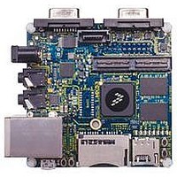
Manufacturer Part Number
MCIMX53-START
Description
KIT DEVELOPMENT I.MX53
Manufacturer
Freescale Semiconductor
Series
i.MX53r
Type
MCUr
Datasheets
1.MCIMX53-START.pdf
(2 pages)
2.MCIMX53-START.pdf
(180 pages)
3.MCIMX53-START.pdf
(204 pages)
Specifications of MCIMX53-START
Contents
Board
Silicon Manufacturer
Freescale
Core Architecture
ARM
Core Sub-architecture
Cortex - A8
Silicon Core Number
I.MX5
Silicon Family Name
I.MX53
Peak Reflow Compatible (260 C)
Yes
Rohs Compliant
Yes
Leaded Process Compatible
Yes
Lead Free Status / RoHS Status
Lead free / RoHS Compliant
For Use With/related Products
i.MX53
Lead Free Status / Rohs Status
Supplier Unconfirmed
Available stocks
Company
Part Number
Manufacturer
Quantity
Price


Electrical Characteristics
4.7.8.5
The IPU Display Interface supports two kinds of display accesses: synchronous and asynchronous. There
are two groups of external interface pins to provide synchronous and asynchronous controls accordantly.
4.7.8.5.1
The synchronous control changes its value as a function of a system or of an external clock. This control
has a permanent period and a permanent wave form.
There are special physical outputs to provide synchronous controls:
The IPU has a system of internal binding counters for internal events (such as HSYNC/VSYCN and so on)
calculation. The internal event (local start point) is synchronized with internal DI_CLK. A suitable control
starts from the local start point with predefined UP and DOWN values to calculate control’s changing
points with half DI_CLK resolution. A full description of the counters system can be found in the IPU
chapter of the i.MX53xD Reference Manual.
4.7.8.5.2
The asynchronous control is a data-oriented signal that changes its value with an output data according to
additional internal flags coming with the data.
There are special physical outputs to provide asynchronous controls, as follows:
86
•
•
•
•
The ipp_disp_clk is a dedicated base synchronous signal that is used to generate a base display
(component, pixel) clock for a display.
The ipp_pin_1– ipp_pin_7 are general purpose synchronous pins, that can be used to provide
HSYNC, VSYNC, DRDY or any else independent signal to a display.
The ipp_d0_cs and ipp_d1_cs pins are dedicated to provide chip select signals to two displays.
The ipp_pin_11– ipp_pin_17 are general purpose asynchronous pins, that can be used to provide
WR. RD, RS or any other data oriented signal to display.
IPU Display Interface Timing
Synchronous Controls
Asynchronous Controls
Table 56
Disp1 port has reduced pinout depending on IOMUXC configuration and
therefore may not support all the above configurations. See the IOMUXC
table for details.
The IPU has independent signal generators for asynchronous signals
toggling. When a DI decides to put a new asynchronous data in the bus, a
new internal start (local start point) is generated. The signals generators
calculate predefined UP and DOWN values to change pins states with half
DI_CLK resolution.
i.MX53xD Applications Processors for Consumer Products, Rev. 1
provides information for both the Disp0 and Disp1 ports. However,
NOTE
NOTE
Freescale Semiconductor
Related parts for MCIMX53-START
Image
Part Number
Description
Manufacturer
Datasheet
Request
R

Part Number:
Description:
MCIMX-LVDS1
Manufacturer:
Freescale Semiconductor
Datasheet:

Part Number:
Description:
Manufacturer:
Freescale Semiconductor, Inc
Datasheet:
Part Number:
Description:
Manufacturer:
Freescale Semiconductor, Inc
Datasheet:
Part Number:
Description:
Manufacturer:
Freescale Semiconductor, Inc
Datasheet:
Part Number:
Description:
Manufacturer:
Freescale Semiconductor, Inc
Datasheet:
Part Number:
Description:
Manufacturer:
Freescale Semiconductor, Inc
Datasheet:
Part Number:
Description:
Manufacturer:
Freescale Semiconductor, Inc
Datasheet:
Part Number:
Description:
Manufacturer:
Freescale Semiconductor, Inc
Datasheet:
Part Number:
Description:
Manufacturer:
Freescale Semiconductor, Inc
Datasheet:
Part Number:
Description:
Manufacturer:
Freescale Semiconductor, Inc
Datasheet:
Part Number:
Description:
Manufacturer:
Freescale Semiconductor, Inc
Datasheet:
Part Number:
Description:
Manufacturer:
Freescale Semiconductor, Inc
Datasheet:
Part Number:
Description:
Manufacturer:
Freescale Semiconductor, Inc
Datasheet:
Part Number:
Description:
Manufacturer:
Freescale Semiconductor, Inc
Datasheet:
Part Number:
Description:
Manufacturer:
Freescale Semiconductor, Inc
Datasheet: