MCIMX53-START Freescale Semiconductor, MCIMX53-START Datasheet - Page 82
MCIMX53-START
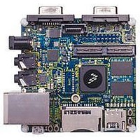
Manufacturer Part Number
MCIMX53-START
Description
KIT DEVELOPMENT I.MX53
Manufacturer
Freescale Semiconductor
Series
i.MX53r
Type
MCUr
Datasheets
1.MCIMX53-START.pdf
(2 pages)
2.MCIMX53-START.pdf
(180 pages)
3.MCIMX53-START.pdf
(204 pages)
Specifications of MCIMX53-START
Contents
Board
Silicon Manufacturer
Freescale
Core Architecture
ARM
Core Sub-architecture
Cortex - A8
Silicon Core Number
I.MX5
Silicon Family Name
I.MX53
Peak Reflow Compatible (260 C)
Yes
Rohs Compliant
Yes
Leaded Process Compatible
Yes
Lead Free Status / RoHS Status
Lead free / RoHS Compliant
For Use With/related Products
i.MX53
Lead Free Status / Rohs Status
Supplier Unconfirmed
Available stocks
Company
Part Number
Manufacturer
Quantity
Price


Electrical Characteristics
SENSB_HSYNC goes to low at the end of line. Pixel clocks then become invalid and the CSI stops
receiving data from the stream. For next line the SENSB_HSYNC timing repeats. For next frame the
SENSB_VSYNC timing repeats.
4.7.8.2.3
The timing is the same as the gated-clock mode (described in
except for the SENSB_HSYNC signal, which is not used (see
valid and cause data to be latched into the input FIFO. The SENSB_PIX_CLK signal is inactive (states
low) until valid data is going to be transmitted over the bus.
The timing described in
different timing. The CSI can be programmed to support rising/falling-edge triggered SENSB_VSYNC;
active-high/low SENSB_HSYNC; and rising/falling-edge triggered SENSB_PIX_CLK.
4.7.8.3
Figure 44
the IPU.
82
SENSB_DATA,
SENSB_VSYNC,
SENSB_HSYNC
SENSB_PIX_CLK
(Sensor Output)
Table 55
SENSB_DATA[19:0]
depicts the sensor interface timing. SENSB_MCLK signal described here is not generated by
SENSB_PIX_CLK
SENSB_VSYNC
Electrical Characteristics
Non-Gated Clock Mode
lists the sensor interface timing characteristics.
Start of Frame
i.MX53xD Applications Processors for Consumer Products, Rev. 1
Figure 43
invalid
Figure 43. Non-Gated Clock Mode Timing Diagram
nth frame
Figure 44. Sensor Interface Timing Diagram
is that of a typical sensor. Some other sensors may have a slightly
1st byte
IP3
IP2
n+1th frame
Section 4.7.8.2.2, “Gated Clock
invalid
Figure
1/IP1
43). All incoming pixel clocks are
1st byte
Freescale Semiconductor
Mode,”)
Related parts for MCIMX53-START
Image
Part Number
Description
Manufacturer
Datasheet
Request
R

Part Number:
Description:
MCIMX-LVDS1
Manufacturer:
Freescale Semiconductor
Datasheet:

Part Number:
Description:
Manufacturer:
Freescale Semiconductor, Inc
Datasheet:
Part Number:
Description:
Manufacturer:
Freescale Semiconductor, Inc
Datasheet:
Part Number:
Description:
Manufacturer:
Freescale Semiconductor, Inc
Datasheet:
Part Number:
Description:
Manufacturer:
Freescale Semiconductor, Inc
Datasheet:
Part Number:
Description:
Manufacturer:
Freescale Semiconductor, Inc
Datasheet:
Part Number:
Description:
Manufacturer:
Freescale Semiconductor, Inc
Datasheet:
Part Number:
Description:
Manufacturer:
Freescale Semiconductor, Inc
Datasheet:
Part Number:
Description:
Manufacturer:
Freescale Semiconductor, Inc
Datasheet:
Part Number:
Description:
Manufacturer:
Freescale Semiconductor, Inc
Datasheet:
Part Number:
Description:
Manufacturer:
Freescale Semiconductor, Inc
Datasheet:
Part Number:
Description:
Manufacturer:
Freescale Semiconductor, Inc
Datasheet:
Part Number:
Description:
Manufacturer:
Freescale Semiconductor, Inc
Datasheet:
Part Number:
Description:
Manufacturer:
Freescale Semiconductor, Inc
Datasheet:
Part Number:
Description:
Manufacturer:
Freescale Semiconductor, Inc
Datasheet: