MCIMX53-START Freescale Semiconductor, MCIMX53-START Datasheet - Page 40
MCIMX53-START
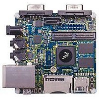
Manufacturer Part Number
MCIMX53-START
Description
KIT DEVELOPMENT I.MX53
Manufacturer
Freescale Semiconductor
Series
i.MX53r
Type
MCUr
Datasheets
1.MCIMX53-START.pdf
(2 pages)
2.MCIMX53-START.pdf
(180 pages)
3.MCIMX53-START.pdf
(204 pages)
Specifications of MCIMX53-START
Contents
Board
Silicon Manufacturer
Freescale
Core Architecture
ARM
Core Sub-architecture
Cortex - A8
Silicon Core Number
I.MX5
Silicon Family Name
I.MX53
Peak Reflow Compatible (260 C)
Yes
Rohs Compliant
Yes
Leaded Process Compatible
Yes
Lead Free Status / RoHS Status
Lead free / RoHS Compliant
For Use With/related Products
i.MX53
Lead Free Status / Rohs Status
Supplier Unconfirmed
Available stocks
Company
Part Number
Manufacturer
Quantity
Price


Electrical Characteristics
Table 23
4.5.3
AC electrical characteristics for LVIO I/O in slow and fast modes are presented in the
Table
in the IOMUXC control registers.
40
1
2
3
1
2
3
4
Single output slew rate
Skew between pad rise/fall asymmetry +
skew caused by SSN
AC input logic high
AC input logic low
AC differential input voltage
Input AC differential cross point voltage
Output AC differential cross point voltage
Single output slew rate
Skew between pad rise/fall asymmetry +
skew caused by SSN
Note that the JEDEC LPDDR2 specification (JESD209_2B) supersedes any specification in this document.
Vid(ac) specifies the input differential voltage |Vtr – Vcp| required for switching, where Vtr is the “true” input signal and Vcp is
the “complementary” input signal. The Minimum value is equal to Vih(ac) – Vil(ac).
The typical value of Vix(ac) is expected to be about 0.5 * OVDD. and Vix(ac) is expected to track variation of OVDD. Vix(ac)
indicates the voltage at which differential input signal must cross.
Note that the JEDEC JESD79_3C specification supersedes any specification in this document.
Vid(ac) specifies the input differential voltage |Vtr-Vcp| required for switching, where Vtr is the “true” input signal and Vcp is
the “complementary” input signal. The Minimum value is equal to Vih(ac) – Vil(ac).
The typical value of Vix(ac) is expected to be about 0.5 * OVDD. and Vix(ac) is expected to track variation of OVDD. Vix(ac)
indicates the voltage at which differential input signal must cross.
The typical value of Vox(ac) is expected to be about 0.5 * OVDD and Vox(ac) is expected to track variation in OVDD. Vox(ac)
indicates the voltage at which differential output signal must cross.
25, respectively. Note that the fast or slow I/O behavior is determined by the appropriate control bit
shows the AC parameters for LPDDR2 I/O operating in DDR3 mode.
LVIO I/O AC Electrical Characteristics
Parameter
Parameter
Table 22. LPDDR2 I/O LPDDR2 mode AC Characteristics
i.MX53xD Applications Processors for Consumer Products, Rev. 1
2
Table 23. LPDDR2 I/O DDR3 mode AC Characteristics
3
4
Symbol
Symbol Test Condition
t
Vox(ac)
Vih(ac)
Vid(ac)
Vix(ac)
SKD
Vil(ac)
tsr
t
SKD
tsr
impedance= 60Ohm
Drive impedance=
At 25 Ω to Vref
Test Condition
50Ohm to Vref.
50Ohm to Vref.
clk=266MHz
clk=400MHz
40Ohm +-30%
5pF load.Drive
clk=266MHz
clk=400MHz
5pF load.
+-30%
—
—
—
—
—
Vref + 0.175
Vref
Vref
0.35
Min
2.5
—
–
–
0
0.15
0.15
Min
1.5
—
1
1
(continued)
Typ
—
—
—
—
—
—
—
1
Typ
—
—
—
Vref
Freescale Semiconductor
Vref + 0.15
Vref + 0.15
OVDD
Table 24
Max
0.2
0.1
–
—
5
0.175
Max
0.2
0.1
3.5
2.5
and
V/ns
Unit
ns
V
V
V
V
V
V/ns
Unit
ns
Related parts for MCIMX53-START
Image
Part Number
Description
Manufacturer
Datasheet
Request
R

Part Number:
Description:
MCIMX-LVDS1
Manufacturer:
Freescale Semiconductor
Datasheet:

Part Number:
Description:
Manufacturer:
Freescale Semiconductor, Inc
Datasheet:
Part Number:
Description:
Manufacturer:
Freescale Semiconductor, Inc
Datasheet:
Part Number:
Description:
Manufacturer:
Freescale Semiconductor, Inc
Datasheet:
Part Number:
Description:
Manufacturer:
Freescale Semiconductor, Inc
Datasheet:
Part Number:
Description:
Manufacturer:
Freescale Semiconductor, Inc
Datasheet:
Part Number:
Description:
Manufacturer:
Freescale Semiconductor, Inc
Datasheet:
Part Number:
Description:
Manufacturer:
Freescale Semiconductor, Inc
Datasheet:
Part Number:
Description:
Manufacturer:
Freescale Semiconductor, Inc
Datasheet:
Part Number:
Description:
Manufacturer:
Freescale Semiconductor, Inc
Datasheet:
Part Number:
Description:
Manufacturer:
Freescale Semiconductor, Inc
Datasheet:
Part Number:
Description:
Manufacturer:
Freescale Semiconductor, Inc
Datasheet:
Part Number:
Description:
Manufacturer:
Freescale Semiconductor, Inc
Datasheet:
Part Number:
Description:
Manufacturer:
Freescale Semiconductor, Inc
Datasheet:
Part Number:
Description:
Manufacturer:
Freescale Semiconductor, Inc
Datasheet: