MCIMX53-START Freescale Semiconductor, MCIMX53-START Datasheet - Page 32
MCIMX53-START
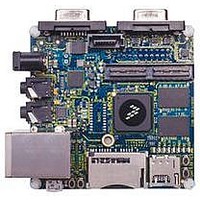
Manufacturer Part Number
MCIMX53-START
Description
KIT DEVELOPMENT I.MX53
Manufacturer
Freescale Semiconductor
Series
i.MX53r
Type
MCUr
Datasheets
1.MCIMX53-START.pdf
(2 pages)
2.MCIMX53-START.pdf
(180 pages)
3.MCIMX53-START.pdf
(204 pages)
Specifications of MCIMX53-START
Contents
Board
Silicon Manufacturer
Freescale
Core Architecture
ARM
Core Sub-architecture
Cortex - A8
Silicon Core Number
I.MX5
Silicon Family Name
I.MX53
Peak Reflow Compatible (260 C)
Yes
Rohs Compliant
Yes
Leaded Process Compatible
Yes
Lead Free Status / RoHS Status
Lead free / RoHS Compliant
For Use With/related Products
i.MX53
Lead Free Status / Rohs Status
Supplier Unconfirmed
Available stocks
Company
Part Number
Manufacturer
Quantity
Price


1
2
3
4
Electrical Characteristics
4.3.3
The parameters in
The LVIO pads operate only as inputs.
1
2
3
4
32
High-Level DC input voltage
Low-Level DC input voltage
Input Hysteresis
Schmitt trigger VT+
Schmitt trigger VT–
Input current (no pull-up/down)
Input current (22 kΩ Pull-up)
Input current (47 kΩ Pull-up)
Input current (100 kΩ Pull-up)
Input current (100 kΩ Pull-down)
Keeper Circuit Resistance
OVDD – I/O power supply (1.425 V–1.575 V for DDR3)
Vref – DDR3
The single-ended signals need to be within the respective limits (Vih(dc) max, Vil(dc) min) for single-ended signals as well as
the limitations for overshoot and undershoot.
Use an off-chip pull resistor of less than 60kΩ to override this keeper.
DC Electrical Characteristics
Overshoot and undershoot conditions (transitions above OVDD and below GND) on switching pads must be held below 0.6 V,
and the duration of the overshoot/undershoot must not exceed 10% of the system clock cycle. Overshoot/undershoot must be
controlled through printed circuit board layout, transmission line impedance matching, signal line termination, or other
methods. Non-compliance to this specification may affect device reliability or cause permanent damage to the device.
To maintain a valid level, the transition edge of the input must sustain a constant slew rate (monotonic) from the current DC
level through to the target DC level, VIL or VIH. Monotonic input transition time is from 0.1 ns to 1 s. VIL and VIH do not apply
when hysteresis is enabled.
Hysteresis of 350 mV is guaranteed over all operating conditions when hysteresis is enabled.
Use an off-chip pull resistor of less than 60kΩ to override this keeper.
Low Voltage I/O (LVIO) DC Parameters
external reference voltage
2, 3
2, 3
Table 14
i.MX53xD Applications Processors for Consumer Products, Rev. 1
1, 2
1, 2
are guaranteed per the operating ranges in
Table 14. LVIO DC Electrical Characteristics
Symbol
VHYS
VT+
VT–
VIH
VIL
IIN
IIN
IIN
IIN
IIN
—
Test Conditions
OVDD = 1.875 V
OVDD = 2.775 V
OVDD = 1.875 V
OVDD = 2.775 V
VI = OVDD
VI = OVDD
VI = OVDD
VI = OVDD
VI = OVDD
VI = 0 V
VI = 0 V
VI = 0 V
VI = 0 V
VI = 0 V
—
—
—
—
0.7 × OVDD
0.5 × OVDD
0.35
Min
Table
—
—
—
—
—
—
—
—
0
6, unless otherwise noted.
125
0.62
1.27
Typ
125
1.7
—
—
—
—
—
—
—
—
4
Freescale Semiconductor
0.3 × OVDD
0.5 × OVDD
OVDD
Max
0.12
0.12
0.12
0.25
250
120
161
76
36
36
—
—
—
—
Unit
nA
μA
μA
μA
μA
kΩ
V
V
V
V
V
Related parts for MCIMX53-START
Image
Part Number
Description
Manufacturer
Datasheet
Request
R

Part Number:
Description:
MCIMX-LVDS1
Manufacturer:
Freescale Semiconductor
Datasheet:

Part Number:
Description:
Manufacturer:
Freescale Semiconductor, Inc
Datasheet:
Part Number:
Description:
Manufacturer:
Freescale Semiconductor, Inc
Datasheet:
Part Number:
Description:
Manufacturer:
Freescale Semiconductor, Inc
Datasheet:
Part Number:
Description:
Manufacturer:
Freescale Semiconductor, Inc
Datasheet:
Part Number:
Description:
Manufacturer:
Freescale Semiconductor, Inc
Datasheet:
Part Number:
Description:
Manufacturer:
Freescale Semiconductor, Inc
Datasheet:
Part Number:
Description:
Manufacturer:
Freescale Semiconductor, Inc
Datasheet:
Part Number:
Description:
Manufacturer:
Freescale Semiconductor, Inc
Datasheet:
Part Number:
Description:
Manufacturer:
Freescale Semiconductor, Inc
Datasheet:
Part Number:
Description:
Manufacturer:
Freescale Semiconductor, Inc
Datasheet:
Part Number:
Description:
Manufacturer:
Freescale Semiconductor, Inc
Datasheet:
Part Number:
Description:
Manufacturer:
Freescale Semiconductor, Inc
Datasheet:
Part Number:
Description:
Manufacturer:
Freescale Semiconductor, Inc
Datasheet:
Part Number:
Description:
Manufacturer:
Freescale Semiconductor, Inc
Datasheet: