MA330013 Microchip Technology, MA330013 Datasheet - Page 152
MA330013
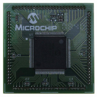
Manufacturer Part Number
MA330013
Description
MODULE PLUG-IN DSPIC33 100TQFP
Manufacturer
Microchip Technology
Specifications of MA330013
Accessory Type
Plug-In Module (PIM) - dsPIC33FJ256MC710
Tool / Board Applications
General Purpose MCU, MPU, DSP, DSC
Mcu Supported Families
DsPIC33
Silicon Manufacturer
Microchip
Core Architecture
DsPIC
Core Sub-architecture
DsPIC33
Silicon Core Number
DsPIC33F
Silicon Family Name
DsPIC33FJxxMCxxx
Rohs Compliant
Yes
For Use With
DM330023 - BOARD DEV DSPICDEM MCHV
Lead Free Status / RoHS Status
Not applicable / Not applicable
For Use With/related Products
Explorer 16 (DM240001 or DM240002)
Lead Free Status / RoHS Status
Lead free / RoHS Compliant, Not applicable / Not applicable


dsPIC33F
8.1
There are seven system clock options provided by the
dsPIC33F:
• FRC Oscillator
• FRC Oscillator with PLL
• Primary (XT, HS or EC) Oscillator
• Primary Oscillator with PLL
• Secondary (LP) Oscillator
• LPRC Oscillator
• FRC Oscillator with postscaler
8.1.1
The FRC (Fast RC) internal oscillator runs at a nominal
frequency of 7.37 MHz. The user software can tune the
FRC frequency. User software can optionally specify a
factor (ranging from 1:2 to 1:256) by which the FRC
clock frequency is divided. This factor is selected using
the FRCDIV<2:0> (CLKDIV<10:8>) bits.
The primary oscillator can use one of the following as
its clock source:
1.
2.
3.
The secondary (LP) oscillator is designed for low power
and uses a 32.768 kHz crystal or ceramic resonator.
The LP oscillator uses the SOSCI and SOSCO pins.
The LPRC (Low-Power RC) internal oscIllator runs at a
nominal frequency of 32.768 kHz. It is also used as a
reference clock by the Watchdog Timer (WDT) and
Fail-Safe Clock Monitor (FSCM).
The clock signals generated by the FRC and primary
oscillators can be optionally applied to an on-chip
Phase Locked Loop (PLL) to provide a wide range of
output
configuration is described in Section 8.1.3 “PLL
Configuration”.
8.1.2
The oscillator source that is used at a device Power-on
Reset event is selected using Configuration bit settings.
The oscillator Configuration bit settings are located in the
Configuration registers in the program memory. (Refer to
Section 23.1 “Configuration Bits” for further details.)
The Initial Oscillator Selection Configuration bits,
FNOSC<2:0> (FOSCSEL<2:0>), and the Primary Oscil-
lator Mode Select Configuration bits, POSCMD<1:0>
DS70165E-page 150
XT (Crystal): Crystals and ceramic resonators in
the range of 3 MHz to 10 MHz. The crystal is
connected to the OSC1 and OSC2 pins.
HS (High-Speed Crystal): Crystals in the range
of 10 MHz to 40 MHz. The crystal is connected
to the OSC1 and OSC2 pins.
EC (External Clock): External clock signal in the
range of 0.8 MHz to 64 MHz. The external clock
signal is directly applied to the OSC1 pin.
frequencies
CPU Clocking System
SYSTEM CLOCK SOURCES
SYSTEM CLOCK SELECTION
for
device
operation.
PLL
Preliminary
(FOSC<1:0>), select the oscillator source that is used at
a Power-on Reset. The FRC primary oscillator is the
default (unprogrammed) selection.
The Configuration bits allow users to choose between
twelve different clock modes, shown in Table 8-1.
The output of the oscillator (or the output of the PLL if
a PLL mode has been selected) F
generate the device instruction clock (F
defines the operating speed of the device, and speeds
up to 40 MHz are supported by the dsPIC33F
architecture.
Instruction execution speed or device operating
frequency, F
EQUATION 8-1:
8.1.3
The primary oscillator and internal FRC oscillator can
optionally use an on-chip PLL to obtain higher speeds
of operation. The PLL provides a significant amount of
flexibility in selecting the device operating speed. A
block diagram of the PLL is shown in Figure 8-2.
The output of the primary oscillator or FRC, denoted as
‘F
... or 33 before being provided to the PLL’s Voltage
Controlled Oscillator (VCO). The input to the VCO must
be selected to be in the range of 0.8 MHz to 8 MHz.
Since the minimum prescale factor is 2, this implies that
F
MHz. The prescale factor ‘N1’ is selected using the
PLLPRE<4:0> bits (CLKDIV<4:0>).
The PLL Feedback Divisor, selected using the
PLLDIV<8:0> bits (PLLFBD<8:0>), provides a factor ‘M’,
by which the input to the VCO is multiplied. This factor
must be selected such that the resulting VCO output
frequency is in the range of 100 MHz to 200 MHz.
The VCO output is further divided by a postscale factor
‘N2’. This factor is selected using the PLLPOST<1:0>
bits (CLKDIV<7:6>). ‘N2’ can be either 2, 4 or 8, and
must be selected such that the PLL output frequency
(F
generates device operating speeds of 6.25-40 MIPS.
For a primary oscillator or FRC oscillator, output ‘F
the PLL output ‘F
EQUATION 8-2:
IN
IN
OSC
’, is divided down by a prescale factor (N1) of 2, 3,
must be chosen to be in the range of 1.6 MHz to 16
) is in the range of 12.5 MHz to 80 MHz, which
PLL CONFIGURATION
CY
F
, is given by:
OSC
OSC
= F
F
’ is given by:
CY
DEVICE OPERATING
FREQUENCY
F
IN
© 2007 Microchip Technology Inc.
OSC
= F
*
(
OSC
N1*N2
CALCULATION
M
/2
OSC
)
is divided by 2 to
CY
). F
IN
CY
’,
Related parts for MA330013
Image
Part Number
Description
Manufacturer
Datasheet
Request
R

Part Number:
Description:
Manufacturer:
Microchip Technology Inc.
Datasheet:
Part Number:
Description:
Manufacturer:
Microchip Technology Inc.
Datasheet:
Part Number:
Description:
Manufacturer:
Microchip Technology Inc.
Datasheet:
Part Number:
Description:
Manufacturer:
Microchip Technology Inc.
Datasheet:
Part Number:
Description:
Manufacturer:
Microchip Technology Inc.
Datasheet:
Part Number:
Description:
Manufacturer:
Microchip Technology Inc.
Datasheet:
Part Number:
Description:
Manufacturer:
Microchip Technology Inc.
Datasheet:
Part Number:
Description:
Manufacturer:
Microchip Technology Inc.
Datasheet: