MA330013 Microchip Technology, MA330013 Datasheet - Page 190
MA330013
Manufacturer Part Number
MA330013
Description
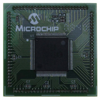
MODULE PLUG-IN DSPIC33 100TQFP
Manufacturer
Microchip Technology
Specifications of MA330013
Accessory Type
Plug-In Module (PIM) - dsPIC33FJ256MC710
Tool / Board Applications
General Purpose MCU, MPU, DSP, DSC
Mcu Supported Families
DsPIC33
Silicon Manufacturer
Microchip
Core Architecture
DsPIC
Core Sub-architecture
DsPIC33
Silicon Core Number
DsPIC33F
Silicon Family Name
DsPIC33FJxxMCxxx
Rohs Compliant
Yes
For Use With
DM330023 - BOARD DEV DSPICDEM MCHV
Lead Free Status / RoHS Status
Not applicable / Not applicable
For Use With/related Products
Explorer 16 (DM240001 or DM240002)
Lead Free Status / RoHS Status
Lead free / RoHS Compliant, Not applicable / Not applicable


dsPIC33F
REGISTER 15-6:
DS70165E-page 188
bit 15
bit 7
Legend:
R = Readable bit
-n = Value at POR
bit 15-12
bit 11-8
bit 7-3
bit 2
bit 1
bit 0
U-0
U-0
—
—
Unimplemented: Read as ‘0’
SEVOPS<3:0>: PWM Special Event Trigger Output Postscale Select bits
1111 = 1:16 postscale
0001 = 1:2 postscale
0000 = 1:1 postscale
Unimplemented: Read as ‘0’
IUE: Immediate Update Enable bit
1 = Updates to the active PDC registers are immediate
0 = Updates to the active PDC registers are synchronized to the PWM time base
OSYNC: Output Override Synchronization bit
1 = Output overrides via the OVDCON register are synchronized to the PWM time base
0 = Output overrides via the OVDCON register occur on next T
UDIS: PWM Update Disable bit
1 = Updates from Duty Cycle and Period Buffer registers are disabled
0 = Updates from Duty Cycle and Period Buffer registers are enabled
•
•
U-0
U-0
—
—
PWMCON2: PWM CONTROL REGISTER 2
W = Writable bit
‘1’ = Bit is set
U-0
U-0
—
—
U-0
U-0
Preliminary
—
—
U = Unimplemented bit, read as ‘0’
‘0’ = Bit is cleared
R/W-0
U-0
—
R/W-0
R/W-0
IUE
CY
SEVOPS<3:0>
boundary
© 2007 Microchip Technology Inc.
x = Bit is unknown
OSYNC
R/W-0
R/W-0
R/W-0
R/W-0
UDIS
bit 8
bit 0
Related parts for MA330013
Image
Part Number
Description
Manufacturer
Datasheet
Request
R

Part Number:
Description:
Manufacturer:
Microchip Technology Inc.
Datasheet:
Part Number:
Description:
Manufacturer:
Microchip Technology Inc.
Datasheet:
Part Number:
Description:
Manufacturer:
Microchip Technology Inc.
Datasheet:
Part Number:
Description:
Manufacturer:
Microchip Technology Inc.
Datasheet:
Part Number:
Description:
Manufacturer:
Microchip Technology Inc.
Datasheet:
Part Number:
Description:
Manufacturer:
Microchip Technology Inc.
Datasheet:
Part Number:
Description:
Manufacturer:
Microchip Technology Inc.
Datasheet:
Part Number:
Description:
Manufacturer:
Microchip Technology Inc.
Datasheet: