MA330013 Microchip Technology, MA330013 Datasheet - Page 342
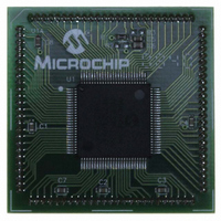
MA330013
Manufacturer Part Number
MA330013
Description
MODULE PLUG-IN DSPIC33 100TQFP
Manufacturer
Microchip Technology
Specifications of MA330013
Accessory Type
Plug-In Module (PIM) - dsPIC33FJ256MC710
Tool / Board Applications
General Purpose MCU, MPU, DSP, DSC
Mcu Supported Families
DsPIC33
Silicon Manufacturer
Microchip
Core Architecture
DsPIC
Core Sub-architecture
DsPIC33
Silicon Core Number
DsPIC33F
Silicon Family Name
DsPIC33FJxxMCxxx
Rohs Compliant
Yes
For Use With
DM330023 - BOARD DEV DSPICDEM MCHV
Lead Free Status / RoHS Status
Not applicable / Not applicable
For Use With/related Products
Explorer 16 (DM240001 or DM240002)
Lead Free Status / RoHS Status
Lead free / RoHS Compliant, Not applicable / Not applicable


dsPIC33F
TABLE 26-37: DCI MODULE (MULTI-CHANNEL, I
DS70165E-page 340
AC CHARACTERISTICS
CS10
CS11
CS20
CS21
CS30
CS31
CS35
CS36
CS40
CS41
CS50
CS51
CS55
CS56
Note 1:
Param
No.
2:
3:
4:
T
T
T
T
T
T
T
T
T
T
T
T
T
T
CSCKL
CSCKH
CSCKF
CSCKR
CSDOF
CSDOR
CSDI
COFSF
COFSR
SCOFS
Symbol
DV
DIV
HCSDI
HCOFS
These parameters are characterized but not tested in manufacturing.
Data in “Typ” column is at 5V, 25°C unless otherwise stated. Parameters are for design guidance only and
are not tested.
The minimum clock period for CSCK is 100 ns. Therefore, the clock generated in Master mode must not
violate this specification.
Assumes 50 pF load on all DCI pins.
CSCK Input Low Time
(CSCK pin is an input)
CSCK Output Low Time
(CSCK pin is an output)
CSCK Input High Time
(CSCK pin is an input)
CSCK Output High Time
(CSCK pin is an output)
CSCK Output Fall Time
(CSCK pin is an output)
CSCK Output Rise Time
(CSCK pin is an output)
CSDO Data Output Fall Time
CSDO Data Output Rise Time
Clock Edge to CSDO Data Valid
Clock Edge to CSDO Tri-Stated
Setup Time of CSDI Data Input to
CSCK Edge (CSCK pin is input
or output)
Hold Time of CSDI Data Input to
CSCK Edge (CSCK pin is input
or output)
COFS Fall Time
(COFS pin is output)
COFS Rise Time
(COFS pin is output)
Setup Time of COFS Data Input
to CSCK Edge (COFS pin is
input)
Hold Time of COFS Data Input to
CSCK Edge (COFS pin is input)
Characteristic
(1)
(4)
(3)
(4)
(3)
(4)
Preliminary
(4)
Standard Operating Conditions: 3.0V to 3.6V
(unless otherwise stated)
Operating temperature
T
T
CY
CY
2
S MODES) TIMING REQUIREMENTS
Min
/2 + 20
/2 + 20
30
30
10
20
20
20
20
—
—
—
—
—
—
—
Typ
—
—
—
—
10
10
10
10
—
—
—
10
10
—
—
—
(2)
Max
-40°C T
—
—
—
—
25
25
25
25
10
20
—
—
25
25
—
—
© 2007 Microchip Technology Inc.
Units
A
ns
ns
ns
ns
ns
ns
ns
ns
ns
ns
ns
ns
ns
ns
ns
ns
+85°C
Note 1
Note 1
Conditions
—
—
—
—
—
—
—
—
—
—
—
—
—
—
Related parts for MA330013
Image
Part Number
Description
Manufacturer
Datasheet
Request
R

Part Number:
Description:
Manufacturer:
Microchip Technology Inc.
Datasheet:
Part Number:
Description:
Manufacturer:
Microchip Technology Inc.
Datasheet:
Part Number:
Description:
Manufacturer:
Microchip Technology Inc.
Datasheet:
Part Number:
Description:
Manufacturer:
Microchip Technology Inc.
Datasheet:
Part Number:
Description:
Manufacturer:
Microchip Technology Inc.
Datasheet:
Part Number:
Description:
Manufacturer:
Microchip Technology Inc.
Datasheet:
Part Number:
Description:
Manufacturer:
Microchip Technology Inc.
Datasheet:
Part Number:
Description:
Manufacturer:
Microchip Technology Inc.
Datasheet: