MA330013 Microchip Technology, MA330013 Datasheet - Page 281
MA330013
Manufacturer Part Number
MA330013
Description
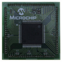
MODULE PLUG-IN DSPIC33 100TQFP
Manufacturer
Microchip Technology
Specifications of MA330013
Accessory Type
Plug-In Module (PIM) - dsPIC33FJ256MC710
Tool / Board Applications
General Purpose MCU, MPU, DSP, DSC
Mcu Supported Families
DsPIC33
Silicon Manufacturer
Microchip
Core Architecture
DsPIC
Core Sub-architecture
DsPIC33
Silicon Core Number
DsPIC33F
Silicon Family Name
DsPIC33FJxxMCxxx
Rohs Compliant
Yes
For Use With
DM330023 - BOARD DEV DSPICDEM MCHV
Lead Free Status / RoHS Status
Not applicable / Not applicable
For Use With/related Products
Explorer 16 (DM240001 or DM240002)
Lead Free Status / RoHS Status
Lead free / RoHS Compliant, Not applicable / Not applicable


REGISTER 22-1:
© 2007 Microchip Technology Inc.
bit 15
bit 7
Legend:
R = Readable bit
-n = Value at POR
bit 15
bit 14
bit 13
bit 12
bit 11
bit 10
bit 9-8
bit 7-5
bit 4
R/W-0
ADON
R/W-0
ADON: ADC Operating Mode bit
1 = ADC module is operating
0 = ADC is off
Unimplemented: Read as ‘0’
ADSIDL: Stop in Idle Mode bit
1 = Discontinue module operation when device enters Idle mode
0 = Continue module operation in Idle mode
ADDMABM: DMA Buffer Build Mode bit
1 = DMA buffers are written in the order of conversion. The module will provide an address to the
0 = DMA buffers are written in Scatter/Gather mode. The module will provide a scatter/gather address
Unimplemented: Read as ‘0’
AD12B: 10-bit or 12-bit Operation Mode bit
1 = 12-bit, 1-channel ADC operation
0 = 10-bit, 4-channel ADC operation
FORM<1:0>: Data Output Format bits
For 10-bit operation:
11 = Signed fractional (D
10 = Fractional (D
01 = Signed integer (D
00 = Integer (D
For 12-bit operation:
11 = Signed fractional (D
10 = Fractional (D
01 = Signed Integer (D
00 = Integer (D
SSRC<2:0>: Sample Clock Source Select bits
111 = Internal counter ends sampling and starts conversion (auto-convert)
110 = Reserved
101 = Reserved
100 = Reserved
011 = MPWM interval ends sampling and starts conversion
010 = GP timer (Timer3 for ADC1, Timer5 for ADC2) compare ends sampling and starts conversion
001 = Active transition on INTx pin ends sampling and starts conversion
000 = Clearing sample bit ends sampling and starts conversion
Unimplemented: Read as ‘0’
SSRC<2:0>
R/W-0
DMA channel that is the same as the address used for the non-DMA stand-alone buffer.
to the DMA channel, based on the index of the analog input and the size of the DMA buffer.
U-0
—
ADxCON1: ADCx CONTROL REGISTER 1 (where x = 1 or 2)
HC = Cleared by hardware
W = Writable bit
‘1’ = Bit is set
OUT
OUT
ADSIDL
R/W-0
R/W-0
OUT
OUT
= 0000 00dd dddd dddd)
= 0000 dddd dddd dddd)
= dddd dddd dd00 0000)
= dddd dddd dddd 0000)
OUT
OUT
OUT
OUT
= ssss sssd dddd dddd, where s = .NOT.d<9>)
= ssss sddd dddd dddd, where s = .NOT.d<11>)
= sddd dddd dd00 0000, where s = .NOT.d<9>)
= sddd dddd dddd 0000, where s = .NOT.d<11>)
ADDMABM
R/W-0
Preliminary
U-0
—
HS = Set by hardware
U = Unimplemented bit, read as ‘0’
‘0’ = Bit is cleared
SIMSAM
R/W-0
U-0
—
AD12B
R/W-0
R/W-0
ASAM
x = Bit is unknown
dsPIC33F
HC,HS
R/W-0
R/W-0
SAMP
FORM<1:0>
DS70165E-page 279
HC, HS
DONE
R/W-0
R/C-0
bit 8
bit 0
Related parts for MA330013
Image
Part Number
Description
Manufacturer
Datasheet
Request
R

Part Number:
Description:
Manufacturer:
Microchip Technology Inc.
Datasheet:
Part Number:
Description:
Manufacturer:
Microchip Technology Inc.
Datasheet:
Part Number:
Description:
Manufacturer:
Microchip Technology Inc.
Datasheet:
Part Number:
Description:
Manufacturer:
Microchip Technology Inc.
Datasheet:
Part Number:
Description:
Manufacturer:
Microchip Technology Inc.
Datasheet:
Part Number:
Description:
Manufacturer:
Microchip Technology Inc.
Datasheet:
Part Number:
Description:
Manufacturer:
Microchip Technology Inc.
Datasheet:
Part Number:
Description:
Manufacturer:
Microchip Technology Inc.
Datasheet: