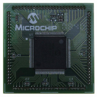
MA330013 Microchip Technology, MA330013 Datasheet - Page 207

MA330013
Manufacturer Part Number
MA330013
Description
MODULE PLUG-IN DSPIC33 100TQFP
Manufacturer
Microchip Technology
Specifications of MA330013
Accessory Type
Plug-In Module (PIM) - dsPIC33FJ256MC710
Tool / Board Applications
General Purpose MCU, MPU, DSP, DSC
Mcu Supported Families
DsPIC33
Silicon Manufacturer
Microchip
Core Architecture
DsPIC
Core Sub-architecture
DsPIC33
Silicon Core Number
DsPIC33F
Silicon Family Name
DsPIC33FJxxMCxxx
Rohs Compliant
Yes
For Use With
DM330023 - BOARD DEV DSPICDEM MCHV
Lead Free Status / RoHS Status
Not applicable / Not applicable
For Use With/related Products
Explorer 16 (DM240001 or DM240002)
Lead Free Status / RoHS Status
Lead free / RoHS Compliant, Not applicable / Not applicable
- Current page: 207 of 370
- Download datasheet (6Mb)
17.0
The Serial Peripheral Interface (SPI) module is a syn-
chronous serial interface useful for communicating with
other peripheral or microcontroller devices. These
peripheral devices may be serial EEPROMs, shift regis-
ters, display drivers, ADC, etc. The SPI module is
compatible with SPI and SIOP from Motorola
Each SPI module consists of a 16-bit shift register,
SPIxSR (where x = 1 or 2), used for shifting data in and
out, and a buffer register, SPIxBUF. A control register,
SPIxCON, configures the module. Additionally, a status
register, SPIxSTAT, indicates various status conditions.
The serial interface consists of 4 pins: SDIx (serial data
input), SDOx (serial data output), SCKx (shift clock input
or output), and SSx (active low slave select).
In Master mode operation, SCK is a clock output but in
Slave mode, it is a clock input.
A series of eight (8) or sixteen (16) clock pulses shift out
bits from the SPIxSR to SDOx pin and simultaneously
shift in data from SDIx pin. An interrupt is generated
when the transfer is complete and the corresponding
interrupt flag bit (SPI1IF or SPI2IF) is set. This interrupt
can be disabled through an interrupt enable bit (SPI1IE
or SPI2IE).
The receive operation is double-buffered. When a com-
plete byte is received, it is transferred from SPIxSR to
SPIxBUF.
If the receive buffer is full when new data is being trans-
ferred from SPIxSR to SPIxBUF, the module will set the
SPIROV bit indicating an overflow condition. The transfer
of the data from SPIxSR to SPIxBUF will not be com-
pleted and the new data will be lost. The module will not
respond to SCL transitions while SPIROV is ‘1’, effec-
tively disabling the module until SPIxBUF is read by user
software.
Transmit writes are also double-buffered. The user writes
to SPIxBUF. When the master or slave transfer is com-
pleted, the contents of the shift register (SPIxSR) are
moved to the receive buffer. If any transmit data has been
written to the buffer register, the contents of the transmit
© 2007 Microchip Technology Inc.
Note:
Note:
SERIAL PERIPHERAL
INTERFACE (SPI)
This data sheet summarizes the features
of this group of dsPIC33F devices. It is not
intended to be a comprehensive reference
source. To complement the information in
this data sheet, refer to the “dsPIC30F
Family Reference Manual” (DS70046).
In this section, the SPI modules are
referred to together as SPIx, or separately
as SPI1 and SPI2. Special Function Reg-
isters will follow a similar notation. For
example, SPIxCON refers to the control
register for the SPI1 or SPI2 module.
®
.
Preliminary
buffer are moved to SPIxSR. The received data is thus
placed in SPIxBUF and the transmit data in SPIxSR is
ready for the next transfer.
To set up the SPI module for the Master mode of
operation:
1.
2.
3.
4.
5.
To set up the SPI module for the Slave mode of operation:
1.
2.
3.
4.
5.
6.
7.
The SPI module generates an interrupt indicating com-
pletion of a byte or word transfer, as well as a separate
interrupt for all SPI error conditions.
Note:
Note:
If using interrupts:
a)
b)
c)
Write the desired settings to the SPIxCON
register with MSTEN (SPIxCON1<5>) = 1.
Clear the SPIROV bit (SPIxSTAT<6>).
Enable SPI operation by setting the SPIEN bit
(SPIxSTAT<15>).
Write the data to be transmitted to the SPIxBUF
register. Transmission (and reception) will start as
soon as data is written to the SPIxBUF register.
Clear the SPIxBUF register.
If using interrupts:
a)
b)
c)
Write the desired settings to the SPIxCON1 and
SPIxCON2
(SPIxCON1<5>) = 0.
Clear the SMP bit.
If the CKE bit is set, then the SSEN bit
(SPIxCON1<7>) must be set to enable the SSx
pin.
Clear the SPIROV bit (SPIxSTAT<6>).
Enable SPI operation by setting the SPIEN bit
(SPIxSTAT<15>).
Clear the SPIxIF bit in the respective IFSn
register.
Set the SPIxIE bit in the respective IECn
register.
Write the SPIxIP bits in the respective IPCn
register to set the interrupt priority.
Clear the SPIxIF bit in the respective IFSn
register.
Set the SPIxIE bit in the respective IECn
register.
Write the SPIxIP bits in the respective IPCn
register to set the interrupt priority.
Both the transmit buffer (SPIxTXB) and
the receive buffer (SPIxRXB) are mapped
to the same register address, SPIxBUF.
Do not perform read-modify-write opera-
tions (such as bit-oriented instructions) on
the SPIxBUF register.
Both SPI1 and SPI2 can trigger a DMA
data transfer. If SPI1 or SPI2 is selected
as the DMA IRQ source, a DMA transfer
occurs when the SPI1IF or SPI2IF bit gets
set as a result of an SPI1 or SPI2 byte or
word transfer.
registers
dsPIC33F
with
DS70165E-page 205
MSTEN
Related parts for MA330013
Image
Part Number
Description
Manufacturer
Datasheet
Request
R

Part Number:
Description:
Manufacturer:
Microchip Technology Inc.
Datasheet:

Part Number:
Description:
Manufacturer:
Microchip Technology Inc.
Datasheet:

Part Number:
Description:
Manufacturer:
Microchip Technology Inc.
Datasheet:

Part Number:
Description:
Manufacturer:
Microchip Technology Inc.
Datasheet:

Part Number:
Description:
Manufacturer:
Microchip Technology Inc.
Datasheet:

Part Number:
Description:
Manufacturer:
Microchip Technology Inc.
Datasheet:

Part Number:
Description:
Manufacturer:
Microchip Technology Inc.
Datasheet:

Part Number:
Description:
Manufacturer:
Microchip Technology Inc.
Datasheet:


