MA330013 Microchip Technology, MA330013 Datasheet - Page 290
MA330013
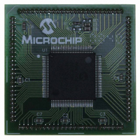
Manufacturer Part Number
MA330013
Description
MODULE PLUG-IN DSPIC33 100TQFP
Manufacturer
Microchip Technology
Specifications of MA330013
Accessory Type
Plug-In Module (PIM) - dsPIC33FJ256MC710
Tool / Board Applications
General Purpose MCU, MPU, DSP, DSC
Mcu Supported Families
DsPIC33
Silicon Manufacturer
Microchip
Core Architecture
DsPIC
Core Sub-architecture
DsPIC33
Silicon Core Number
DsPIC33F
Silicon Family Name
DsPIC33FJxxMCxxx
Rohs Compliant
Yes
For Use With
DM330023 - BOARD DEV DSPICDEM MCHV
Lead Free Status / RoHS Status
Not applicable / Not applicable
For Use With/related Products
Explorer 16 (DM240001 or DM240002)
Lead Free Status / RoHS Status
Lead free / RoHS Compliant, Not applicable / Not applicable


dsPIC33F
REGISTER 22-9:
REGISTER 22-10: ADxPCFGL: ADCx PORT CONFIGURATION REGISTER LOW
DS70165E-page 288
bit 15
bit 7
Legend:
R = Readable bit
-n = Value at POR
bit 15-0
Note 1:
bit 15
bit 7
Legend:
R = Readable bit
-n = Value at POR
bit 15-0
Note 1:
PCFG31
PCFG23
PCFG15
PCFG7
R/W-0
R/W-0
R/W-0
R/W-0
2:
2:
On devices without 32 analog inputs, all PCFG bits are R/W by user. However, PCFG bits are ignored on
ports without a corresponding input on device.
ADC2 only supports analog inputs AN0-AN15; therefore, no ADC2 port Configuration register exists.
On devices without 16 analog inputs, all PCFG bits are R/W by user. However, PCFG bits are ignored on
ports without a corresponding input on device.
On devices with two analog-to-digital modules, both AD1PCFGL and AD2PCFGL will affect the
configuration of port pins multiplexed with AN0-AN15.
PCFG<31:16>: ADC Port Configuration Control bits
1 = Port pin in Digital mode, port read input enabled, ADC input multiplexor connected to AV
0 = Port pin in Analog mode, port read input disabled, ADC samples pin voltage
PCFG<15:0>: ADC Port Configuration Control bits
1 = Port pin in Digital mode, port read input enabled, ADC input multiplexor connected to AV
0 = Port pin in Analog mode, port read input disabled, ADC samples pin voltage
PCFG30
PCFG22
PCFG14
PCFG6
R/W-0
R/W-0
R/W-0
R/W-0
AD1PCFGH: ADC1 PORT CONFIGURATION REGISTER HIGH
W = Writable bit
W = Writable bit
‘1’ = Bit is set
‘1’ = Bit is set
PCFG29
PCFG21
PCFG13
PCFG5
R/W-0
R/W-0
R/W-0
R/W-0
PCFG28
PCFG20
PCFG12
PCFG4
R/W-0
R/W-0
R/W-0
R/W-0
Preliminary
U = Unimplemented bit, read as ‘0’
U = Unimplemented bit, read as ‘0’
‘0’ = Bit is cleared
‘0’ = Bit is cleared
PCFG27
PCFG19
PCFG11
PCFG3
R/W-0
R/W-0
R/W-0
R/W-0
PCFG26
PCFG18
PCFG10
PCFG2
R/W-0
R/W-0
R/W-0
R/W-0
© 2007 Microchip Technology Inc.
x = Bit is unknown
x = Bit is unknown
PCFG25
PCFG17
PCFG9
PCFG1
R/W-0
R/W-0
R/W-0
R/W-0
(1,2)
(1,2)
PCFG24
PCFG16
PCFG8
PCFG0
R/W-0
R/W-0
R/W-0
R/W-0
SS
SS
bit 8
bit 0
bit 8
bit 0
Related parts for MA330013
Image
Part Number
Description
Manufacturer
Datasheet
Request
R

Part Number:
Description:
Manufacturer:
Microchip Technology Inc.
Datasheet:
Part Number:
Description:
Manufacturer:
Microchip Technology Inc.
Datasheet:
Part Number:
Description:
Manufacturer:
Microchip Technology Inc.
Datasheet:
Part Number:
Description:
Manufacturer:
Microchip Technology Inc.
Datasheet:
Part Number:
Description:
Manufacturer:
Microchip Technology Inc.
Datasheet:
Part Number:
Description:
Manufacturer:
Microchip Technology Inc.
Datasheet:
Part Number:
Description:
Manufacturer:
Microchip Technology Inc.
Datasheet:
Part Number:
Description:
Manufacturer:
Microchip Technology Inc.
Datasheet: