MA330013 Microchip Technology, MA330013 Datasheet - Page 263
MA330013
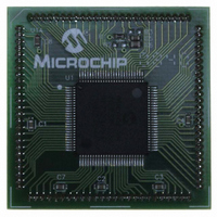
Manufacturer Part Number
MA330013
Description
MODULE PLUG-IN DSPIC33 100TQFP
Manufacturer
Microchip Technology
Specifications of MA330013
Accessory Type
Plug-In Module (PIM) - dsPIC33FJ256MC710
Tool / Board Applications
General Purpose MCU, MPU, DSP, DSC
Mcu Supported Families
DsPIC33
Silicon Manufacturer
Microchip
Core Architecture
DsPIC
Core Sub-architecture
DsPIC33
Silicon Core Number
DsPIC33F
Silicon Family Name
DsPIC33FJxxMCxxx
Rohs Compliant
Yes
For Use With
DM330023 - BOARD DEV DSPICDEM MCHV
Lead Free Status / RoHS Status
Not applicable / Not applicable
For Use With/related Products
Explorer 16 (DM240001 or DM240002)
Lead Free Status / RoHS Status
Lead free / RoHS Compliant, Not applicable / Not applicable


21.0
21.1
The dsPIC33F Data Converter Interface (DCI) module
allows simple interfacing of devices, such as audio
coder/decoders (Codecs), ADC and D/A converters.
The following interfaces are supported:
• Framed Synchronous Serial Transfer (Single or
• Inter-IC Sound (I
• AC-Link Compliant mode
The DCI module provides the following general
features:
• Programmable word size up to 16 bits
• Supports up to 16 time slots, for a maximum
• Data buffering for up to 4 samples without CPU
21.2
There are four I/O pins associated with the module.
When enabled, the module controls the data direction
of each of the four pins.
21.2.1
The CSCK pin provides the serial clock for the DCI
module. The CSCK pin may be configured as an input
or output using the CSCKD control bit in the DCICON1
SFR. When configured as an output, the serial clock is
provided by the dsPIC33F. When configured as an
input, the serial clock must be provided by an external
device.
21.2.2
The Serial Data Output (CSDO) pin is configured as an
output only pin when the module is enabled. The
CSDO pin drives the serial bus whenever data is to be
transmitted. The CSDO pin is tri-stated, or driven to ‘0’,
during CSCK periods when data is not transmitted
depending on the state of the CSDOM control bit. This
allows other devices to place data on the serial bus
during transmission periods not used by the DCI
module.
© 2007 Microchip Technology Inc.
Note:
Multi-Channel)
frame size of 256 bits
overhead
DATA CONVERTER
INTERFACE (DCI) MODULE
Module Introduction
Module I/O Pins
This data sheet summarizes the features
of this group of dsPIC33F devices. It is not
intended to be a comprehensive reference
source. To complement the information in
this data sheet, refer to the “dsPIC30F
Family Reference Manual” (DS70046).
CSCK PIN
CSDO PIN
2
S) Interface
Preliminary
21.2.3
The Serial Data Input (CSDI) pin is configured as an
input only pin when the module is enabled.
21.2.3.1
The Codec Frame Synchronization (COFS) pin is used
to synchronize data transfers that occur on the CSDO
and CSDI pins. The COFS pin may be configured as an
input or an output. The data direction for the COFS pin
is determined by the COFSD control bit in the
DCICON1 register.
The DCI module accesses the shadow registers while
the CPU is in the process of accessing the memory
mapped buffer registers.
21.2.4
Data values are always stored left justified in the
buffers since most Codec data is represented as a
signed 2’s complement fractional number. If the
received word length is less than 16 bits, the unused
Least Significant bits in the Receive Buffer registers are
set to ‘0’ by the module. If the transmitted word length
is less than 16 bits, the unused LSbs in the Transmit
Buffer register are ignored by the module. The word
length setup is described in subsequent sections of this
document.
21.2.5
The DCI module has a 16-bit shift register for shifting
serial data in and out of the module. Data is shifted in/
out of the shift register, MSb first, since audio PCM data
is transmitted in signed 2’s complement format.
21.2.6
The DCI module contains a buffer control unit for
transferring data between the shadow buffer memory
and the Serial Shift register. The buffer control unit is a
simple 2-bit address counter that points to word loca-
tions in the shadow buffer memory. For the receive
memory space (high address portion of DCI buffer
memory), the address counter is concatenated with a
‘0’ in the MSb location to form a 3-bit address. For the
transmit memory space (high portion of DCI buffer
memory), the address counter is concatenated with a
‘1’ in the MSb location.
Note:
CSDI PIN
BUFFER DATA ALIGNMENT
TRANSMIT/RECEIVE SHIFT
REGISTER
DCI BUFFER CONTROL
The DCI buffer control unit always
accesses the same relative location in the
transmit and receive buffers, so only one
address counter is provided.
COFS Pin
dsPIC33F
DS70165E-page 261
Related parts for MA330013
Image
Part Number
Description
Manufacturer
Datasheet
Request
R

Part Number:
Description:
Manufacturer:
Microchip Technology Inc.
Datasheet:
Part Number:
Description:
Manufacturer:
Microchip Technology Inc.
Datasheet:
Part Number:
Description:
Manufacturer:
Microchip Technology Inc.
Datasheet:
Part Number:
Description:
Manufacturer:
Microchip Technology Inc.
Datasheet:
Part Number:
Description:
Manufacturer:
Microchip Technology Inc.
Datasheet:
Part Number:
Description:
Manufacturer:
Microchip Technology Inc.
Datasheet:
Part Number:
Description:
Manufacturer:
Microchip Technology Inc.
Datasheet:
Part Number:
Description:
Manufacturer:
Microchip Technology Inc.
Datasheet: