MA330013 Microchip Technology, MA330013 Datasheet - Page 76
MA330013
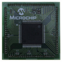
Manufacturer Part Number
MA330013
Description
MODULE PLUG-IN DSPIC33 100TQFP
Manufacturer
Microchip Technology
Specifications of MA330013
Accessory Type
Plug-In Module (PIM) - dsPIC33FJ256MC710
Tool / Board Applications
General Purpose MCU, MPU, DSP, DSC
Mcu Supported Families
DsPIC33
Silicon Manufacturer
Microchip
Core Architecture
DsPIC
Core Sub-architecture
DsPIC33
Silicon Core Number
DsPIC33F
Silicon Family Name
DsPIC33FJxxMCxxx
Rohs Compliant
Yes
For Use With
DM330023 - BOARD DEV DSPICDEM MCHV
Lead Free Status / RoHS Status
Not applicable / Not applicable
For Use With/related Products
Explorer 16 (DM240001 or DM240002)
Lead Free Status / RoHS Status
Lead free / RoHS Compliant, Not applicable / Not applicable


dsPIC33F
3.6.2
The TBLRDL and TBLWTL instructions offer a direct
method of reading or writing the lower word of any
address within the program space without going
through data space. The TBLRDH and TBLWTH instruc-
tions are the only method to read or write the upper
8 bits of a program space word as data.
The PC is incremented by two for each successive
24-bit program word. This allows program memory
addresses to directly map to data space addresses.
Program memory can thus be regarded as two 16-bit
word wide address spaces, residing side by side, each
with the same address range. TBLRDL and TBLWTL
access the space which contains the least significant
data word and TBLRDH and TBLWTH access the space
which contains the upper data byte.
Two table instructions are provided to move byte or
word sized (16-bit) data to and from program space.
Both function as either byte or word operations.
1.
FIGURE 3-10:
DS70165E-page 74
TBLRDL (Table Read Low): In Word mode, it
maps the lower word of the program space
location (P<15:0>) to a data address (D<15:0>).
In Byte mode, either the upper or lower byte of
the lower program word is mapped to the lower
byte of a data address. The upper byte is
selected when Byte Select is ‘1’; the lower byte
is selected when it is ‘0’.
TBLPAG
02
DATA ACCESS FROM PROGRAM
MEMORY USING TABLE
INSTRUCTIONS
23
ACCESSING PROGRAM MEMORY WITH TABLE INSTRUCTIONS
15
0
0x000000
0x020000
0x030000
0x800000
Program Space
Preliminary
The address for the table operation is determined by the data EA
within the page defined by the TBLPAG register.
Only read operations are shown; write operations are also valid in
the user memory area.
TBLRDH.B (Wn<0> = 0)
TBLRDL.B (Wn<0> = 1)
TBLRDL.B (Wn<0> = 0)
TBLRDL.W
2.
In a similar fashion, two table instructions, TBLWTH
and TBLWTL, are used to write individual bytes or
words to a program space address. The details of
their operation are explained in Section 4.0 “Flash
Program Memory”.
For all table operations, the area of program memory
space to be accessed is determined by the Table Page
register (TBLPAG). TBLPAG covers the entire program
memory space of the device, including user and config-
uration spaces. When TBLPAG<7> = 0, the table page
is located in the user memory space. When
TBLPAG<7> = 1, the page is located in configuration
space.
‘Phantom’ Byte
00000000
00000000
00000000
00000000
TBLRDH (Table Read High): In Word mode, it
maps the entire upper word of a program address
(P<23:16>) to a data address. Note that
D<15:8>, the ‘phantom byte’, will always be ‘0’.
In Byte mode, it maps the upper or lower byte of
the program word to D<7:0> of the data
address, as above. Note that the data will
always be ‘0’ when the upper ‘phantom’ byte is
selected (Byte Select = 1).
23
16
© 2007 Microchip Technology Inc.
8
0
Related parts for MA330013
Image
Part Number
Description
Manufacturer
Datasheet
Request
R

Part Number:
Description:
Manufacturer:
Microchip Technology Inc.
Datasheet:
Part Number:
Description:
Manufacturer:
Microchip Technology Inc.
Datasheet:
Part Number:
Description:
Manufacturer:
Microchip Technology Inc.
Datasheet:
Part Number:
Description:
Manufacturer:
Microchip Technology Inc.
Datasheet:
Part Number:
Description:
Manufacturer:
Microchip Technology Inc.
Datasheet:
Part Number:
Description:
Manufacturer:
Microchip Technology Inc.
Datasheet:
Part Number:
Description:
Manufacturer:
Microchip Technology Inc.
Datasheet:
Part Number:
Description:
Manufacturer:
Microchip Technology Inc.
Datasheet: