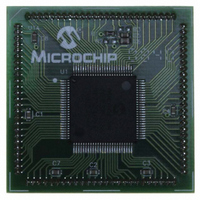
MA330013 Microchip Technology, MA330013 Datasheet - Page 271

MA330013
Manufacturer Part Number
MA330013
Description
MODULE PLUG-IN DSPIC33 100TQFP
Manufacturer
Microchip Technology
Specifications of MA330013
Accessory Type
Plug-In Module (PIM) - dsPIC33FJ256MC710
Tool / Board Applications
General Purpose MCU, MPU, DSP, DSC
Mcu Supported Families
DsPIC33
Silicon Manufacturer
Microchip
Core Architecture
DsPIC
Core Sub-architecture
DsPIC33
Silicon Core Number
DsPIC33F
Silicon Family Name
DsPIC33FJxxMCxxx
Rohs Compliant
Yes
For Use With
DM330023 - BOARD DEV DSPICDEM MCHV
Lead Free Status / RoHS Status
Not applicable / Not applicable
For Use With/related Products
Explorer 16 (DM240001 or DM240002)
Lead Free Status / RoHS Status
Lead free / RoHS Compliant, Not applicable / Not applicable
- Current page: 271 of 370
- Download datasheet (6Mb)
21.6.2
The 20-bit AC-Link mode allows all bits in the data time
slots to be transmitted and received but does not main-
tain data alignment in the TXBUF and RXBUF
registers.
The 20-bit AC-Link mode functions similar to the Multi-
Channel mode of the DCI module, except for the duty
cycle of the frame synchronization signal. The AC-Link
frame synchronization signal should remain high for
16 CSCK cycles and should be low for the following
240 cycles.
The 20-bit mode treats each 256-bit AC-Link frame as
sixteen, 16-bit time slots. In the 20-bit AC-Link mode,
the module operates as if COFSG<3:0> = 1111 and
WS<3:0> = 1111. The data alignment for 20-bit data
slots is ignored. For example, an entire AC-Link data
frame can be transmitted and received in a packed
fashion by setting all bits in the TSCON and RSCON
SFRs. Since the total available buffer length is 64 bits,
it would take 4 consecutive interrupts to transfer the
AC-Link frame. The application software must keep
track of the current AC-Link frame segment.
21.7
The DCI module is configured for I
a value of ‘01’ to the COFSM<1:0> control bits in the
DCICON1 SFR. When operating in the I
DCI module will generate frame synchronization sig-
nals with a 50% duty cycle. Each edge of the frame
synchronization signal marks the boundary of a new
data word transfer.
The user must also select the frame length and data
word size using the COFSG and WS control bits in the
DCICON2 SFR.
© 2007 Microchip Technology Inc.
I
2
S Mode Operation
20-BIT AC-LINK MODE
2
S mode by writing
2
S mode, the
Preliminary
21.7.1
The WS and COFSG control bits are set to produce the
period for one half of an I
frame length is the total number of CSCK cycles
required for a left or right data word transfer.
The BLEN bits must be set for the desired buffer length.
Setting BLEN<1:0> = 01 will produce a CPU interrupt,
once per I
21.7.2
As per the I
default, begin one CSCK cycle after a transition of the
WS signal. A ‘Most Significant bit left justified’ option
can be selected using the DJST control bit in the
DCICON1 SFR.
If DJST = 1, the I
justified. The MSb of the data word will be presented on
the CSDO pin during the same CSCK cycle as the
rising or falling edge of the COFS signal. The CSDO
pin is tri-stated after the data word has been sent.
2
S frame.
2
I
LENGTH SELECTION
I
S specification, a data word transfer will, by
2
2
S FRAME AND DATA WORD
S DATA JUSTIFICATION
2
S data transfers will be MSb left
2
S data frame. That is, the
dsPIC33F
DS70165E-page 269
Related parts for MA330013
Image
Part Number
Description
Manufacturer
Datasheet
Request
R

Part Number:
Description:
Manufacturer:
Microchip Technology Inc.
Datasheet:

Part Number:
Description:
Manufacturer:
Microchip Technology Inc.
Datasheet:

Part Number:
Description:
Manufacturer:
Microchip Technology Inc.
Datasheet:

Part Number:
Description:
Manufacturer:
Microchip Technology Inc.
Datasheet:

Part Number:
Description:
Manufacturer:
Microchip Technology Inc.
Datasheet:

Part Number:
Description:
Manufacturer:
Microchip Technology Inc.
Datasheet:

Part Number:
Description:
Manufacturer:
Microchip Technology Inc.
Datasheet:

Part Number:
Description:
Manufacturer:
Microchip Technology Inc.
Datasheet:


