MA330013 Microchip Technology, MA330013 Datasheet - Page 82
MA330013
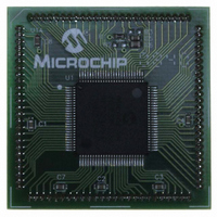
Manufacturer Part Number
MA330013
Description
MODULE PLUG-IN DSPIC33 100TQFP
Manufacturer
Microchip Technology
Specifications of MA330013
Accessory Type
Plug-In Module (PIM) - dsPIC33FJ256MC710
Tool / Board Applications
General Purpose MCU, MPU, DSP, DSC
Mcu Supported Families
DsPIC33
Silicon Manufacturer
Microchip
Core Architecture
DsPIC
Core Sub-architecture
DsPIC33
Silicon Core Number
DsPIC33F
Silicon Family Name
DsPIC33FJxxMCxxx
Rohs Compliant
Yes
For Use With
DM330023 - BOARD DEV DSPICDEM MCHV
Lead Free Status / RoHS Status
Not applicable / Not applicable
For Use With/related Products
Explorer 16 (DM240001 or DM240002)
Lead Free Status / RoHS Status
Lead free / RoHS Compliant, Not applicable / Not applicable


dsPIC33F
4.4.1
The user can program one row of program Flash
memory at a time. To do this, it is necessary to erase
the 8-row erase page that contains the desired row.
The general process is:
1.
2.
3.
EXAMPLE 4-1:
DS70165E-page 80
; Set up NVMCON for block erase operation
; Init pointer to row to be ERASED
Read
(512 instructions) and store in data RAM.
Update the program data in RAM with the
desired new data.
Erase the block (see Example 4-1):
a)
b)
c)
d)
e)
Set the NVMOP bits (NVMCON<3:0>) to
‘0010’ to configure for block erase. Set the
ERASE (NVMCON<6>) and WREN (NVM-
CON<14>) bits.
Write the starting address of the page to be
erased into the TBLPAG and W registers.
Write 55h to NVMKEY.
Write AAh to NVMKEY.
Set the WR bit (NVMCON<15>). The erase
cycle begins and the CPU stalls for the dura-
tion of the erase cycle. When the erase is
done, the WR bit is cleared automatically.
MOV
MOV
MOV
MOV
MOV
TBLWTL W0, [W0]
DISI
MOV
MOV
MOV
MOV
BSET
NOP
NOP
PROGRAMMING ALGORITHM FOR
FLASH PROGRAM MEMORY
eight
#0x4042, W0
W0, NVMCON
#tblpage(PROG_ADDR), W0
W0, TBLPAG
#tbloffset(PROG_ADDR), W0
#5
#0x55, W0
W0, NVMKEY
#0xAA, W1
W1, NVMKEY
NVMCON, #WR
rows
ERASING A PROGRAM MEMORY PAGE
of
program
memory
Preliminary
;
; Initialize NVMCON
;
; Initialize PM Page Boundary SFR
; Initialize in-page EA[15:0] pointer
; Set base address of erase block
; Block all interrupts with priority <7
; for next 5 instructions
; Write the 55 key
;
; Write the AA key
; Start the erase sequence
; Insert two NOPs after the erase
; command is asserted
4.
5.
6.
For protection against accidental operations, the write
initiate sequence for NVMKEY must be used to allow
any erase or program operation to proceed. After the
programming command has been executed, the user
must wait for the programming time until programming
is complete. The two instructions following the start of
the programming sequence should be NOPs, as shown
in Example 4-3.
Write the first 64 instructions from data RAM into
the program memory buffers (see Example 4-2).
Write the program block to Flash memory:
a)
b)
c)
d)
Repeat steps 4 and 5, using the next available
64 instructions from the block in data RAM by
incrementing the value in TBLPAG, until all
512 instructions are written back to Flash memory.
Set the NVMOP bits to ‘0001’ to configure
for row programming. Clear the ERASE bit
and set the WREN bit.
Write 55h to NVMKEY.
Write AAh to NVMKEY.
Set the WR bit. The programming cycle
begins and the CPU stalls for the duration of
the write cycle. When the write to Flash mem-
ory is done, the WR bit is cleared
automatically.
© 2007 Microchip Technology Inc.
Related parts for MA330013
Image
Part Number
Description
Manufacturer
Datasheet
Request
R

Part Number:
Description:
Manufacturer:
Microchip Technology Inc.
Datasheet:
Part Number:
Description:
Manufacturer:
Microchip Technology Inc.
Datasheet:
Part Number:
Description:
Manufacturer:
Microchip Technology Inc.
Datasheet:
Part Number:
Description:
Manufacturer:
Microchip Technology Inc.
Datasheet:
Part Number:
Description:
Manufacturer:
Microchip Technology Inc.
Datasheet:
Part Number:
Description:
Manufacturer:
Microchip Technology Inc.
Datasheet:
Part Number:
Description:
Manufacturer:
Microchip Technology Inc.
Datasheet:
Part Number:
Description:
Manufacturer:
Microchip Technology Inc.
Datasheet: