MA330013 Microchip Technology, MA330013 Datasheet - Page 171
MA330013
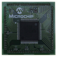
Manufacturer Part Number
MA330013
Description
MODULE PLUG-IN DSPIC33 100TQFP
Manufacturer
Microchip Technology
Specifications of MA330013
Accessory Type
Plug-In Module (PIM) - dsPIC33FJ256MC710
Tool / Board Applications
General Purpose MCU, MPU, DSP, DSC
Mcu Supported Families
DsPIC33
Silicon Manufacturer
Microchip
Core Architecture
DsPIC
Core Sub-architecture
DsPIC33
Silicon Core Number
DsPIC33F
Silicon Family Name
DsPIC33FJxxMCxxx
Rohs Compliant
Yes
For Use With
DM330023 - BOARD DEV DSPICDEM MCHV
Lead Free Status / RoHS Status
Not applicable / Not applicable
For Use With/related Products
Explorer 16 (DM240001 or DM240002)
Lead Free Status / RoHS Status
Lead free / RoHS Compliant, Not applicable / Not applicable


13.0
The input capture module is useful in applications
requiring frequency (period) and pulse measurement.
The dsPIC33F devices support up to eight input
capture channels.
The input capture module captures the 16-bit value of
the selected Time Base register when an event occurs
at the ICx pin. The events that cause a capture event
are listed below in three categories:
1.
2.
3.
FIGURE 13-1:
© 2007 Microchip Technology Inc.
Note:
Note: An ‘x’ in a signal, register or bit name denotes the number of the capture channel.
-Capture timer value on every 4th rising edge
-Capture timer value on every 16th rising
ICx Pin
Simple Capture Event modes
-Capture timer value on every falling edge of
-Capture timer value on every rising edge of
Capture timer value on every edge (rising and
falling)
Prescaler Capture Event modes
input at ICx pin
input at ICx pin
of input at ICx pin
edge of input at ICx pin
INPUT CAPTURE
This data sheet summarizes the features
of this group of dsPIC33F devices. It is not
intended to be a comprehensive reference
source. To complement the information in
this data sheet, refer to the “dsPIC30F
Family Reference Manual” (DS70046).
Prescaler
(1, 4, 16)
Counter
3
INPUT CAPTURE BLOCK DIAGRAM
System Bus
ICxCON
ICM<2:0> (ICxCON<2:0>)
ICOV, ICBNE (ICxCON<4:3>)
Mode Select
Edge Detection Logic
Clock Synchronizer
ICxI<1:0>
and
Preliminary
(in IFSn Register)
Set Flag ICxIF
Interrupt
Logic
Each input capture channel can select between one of
two 16-bit timers (Timer2 or Timer3) for the time base.
The selected timer can use either an internal or
external clock.
Other operational features include:
• Device wake-up from capture pin during CPU
• Interrupt on input capture event
• 4-word FIFO buffer for capture values
• Input capture can also be used to provide
Sleep and Idle modes
- Interrupt optionally generated after 1, 2, 3 or
additional sources of external interrupts
Note:
4 buffer locations are filled
Logic
FIFO
R/W
Only IC1 and IC2 can trigger a DMA data
transfer. If DMA data transfers are
required, the FIFO buffer size must be set
to 1 (ICI<1:0> = 00).
From 16-bit Timers
TMRy TMRz
dsPIC33F
1
ICxBUF
16
0
DS70165E-page 169
16
ICTMR
(ICxCON<7>)
Related parts for MA330013
Image
Part Number
Description
Manufacturer
Datasheet
Request
R

Part Number:
Description:
Manufacturer:
Microchip Technology Inc.
Datasheet:
Part Number:
Description:
Manufacturer:
Microchip Technology Inc.
Datasheet:
Part Number:
Description:
Manufacturer:
Microchip Technology Inc.
Datasheet:
Part Number:
Description:
Manufacturer:
Microchip Technology Inc.
Datasheet:
Part Number:
Description:
Manufacturer:
Microchip Technology Inc.
Datasheet:
Part Number:
Description:
Manufacturer:
Microchip Technology Inc.
Datasheet:
Part Number:
Description:
Manufacturer:
Microchip Technology Inc.
Datasheet:
Part Number:
Description:
Manufacturer:
Microchip Technology Inc.
Datasheet: