MA330013 Microchip Technology, MA330013 Datasheet - Page 47
MA330013
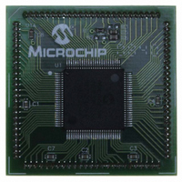
Manufacturer Part Number
MA330013
Description
MODULE PLUG-IN DSPIC33 100TQFP
Manufacturer
Microchip Technology
Specifications of MA330013
Accessory Type
Plug-In Module (PIM) - dsPIC33FJ256MC710
Tool / Board Applications
General Purpose MCU, MPU, DSP, DSC
Mcu Supported Families
DsPIC33
Silicon Manufacturer
Microchip
Core Architecture
DsPIC
Core Sub-architecture
DsPIC33
Silicon Core Number
DsPIC33F
Silicon Family Name
DsPIC33FJxxMCxxx
Rohs Compliant
Yes
For Use With
DM330023 - BOARD DEV DSPICDEM MCHV
Lead Free Status / RoHS Status
Not applicable / Not applicable
For Use With/related Products
Explorer 16 (DM240001 or DM240002)
Lead Free Status / RoHS Status
Lead free / RoHS Compliant, Not applicable / Not applicable


3.2.5
The core has two data spaces, X and Y. These data
spaces can be considered either separate (for some
DSP instructions), or as one unified linear address
range (for MCU instructions). The data spaces are
accessed using two Address Generation Units (AGUs)
and separate data paths. This feature allows certain
instructions to concurrently fetch two words from RAM,
thereby enabling efficient execution of DSP algorithms
such as Finite Impulse Response (FIR) filtering and
Fast Fourier Transform (FFT).
The X data space is used by all instructions and
supports all addressing modes. There are separate
read and write data buses for X data space. The X read
data bus is the read data path for all instructions that
view data space as combined X and Y address space.
It is also the X data prefetch path for the dual operand
DSP instructions (MAC class).
The Y data space is used in concert with the X data
space by the MAC class of instructions (CLR, ED,
EDAC, MAC, MOVSAC, MPY, MPY.N and MSC) to
provide two concurrent data read paths.
Both the X and Y data spaces support Modulo
Addressing mode for all instructions, subject to
addressing mode restrictions. Bit-Reversed Addressing
mode is only supported for writes to X data space.
All data memory writes, including in DSP instructions,
view data space as combined X and Y address space.
The boundary between the X and Y data spaces is
device-dependent and is not user-programmable.
All effective addresses are 16 bits wide and point to
bytes within the data space. Therefore, the data space
address range is 64 Kbytes, or 32K words, though the
implemented memory locations vary by device.
© 2007 Microchip Technology Inc.
X AND Y DATA SPACES
Preliminary
3.2.6
Every dsPIC33F device contains 2 Kbytes of dual ported
DMA RAM located at the end of Y data space. Memory
locations is part of Y data RAM and is in the DMA RAM
space are accessible simultaneously by the CPU and
the DMA controller module. DMA RAM is utilized by the
DMA controller to store data to be transferred to various
peripherals using DMA, as well as data transferred from
various peripherals using DMA. The DMA RAM can be
accessed by the DMA controller without having to steal
cycles from the CPU.
When the CPU and the DMA controller attempt to
concurrently write to the same DMA RAM location, the
hardware ensures that the CPU is given precedence in
accessing the DMA RAM location. Therefore, the DMA
RAM provides a reliable means of transferring DMA
data without ever having to stall the CPU.
Note:
DMA RAM
DMA RAM can be used for general
purpose data storage if the DMA function
is not required in an application.
dsPIC33F
DS70165E-page 45
Related parts for MA330013
Image
Part Number
Description
Manufacturer
Datasheet
Request
R

Part Number:
Description:
Manufacturer:
Microchip Technology Inc.
Datasheet:
Part Number:
Description:
Manufacturer:
Microchip Technology Inc.
Datasheet:
Part Number:
Description:
Manufacturer:
Microchip Technology Inc.
Datasheet:
Part Number:
Description:
Manufacturer:
Microchip Technology Inc.
Datasheet:
Part Number:
Description:
Manufacturer:
Microchip Technology Inc.
Datasheet:
Part Number:
Description:
Manufacturer:
Microchip Technology Inc.
Datasheet:
Part Number:
Description:
Manufacturer:
Microchip Technology Inc.
Datasheet:
Part Number:
Description:
Manufacturer:
Microchip Technology Inc.
Datasheet: