MA330013 Microchip Technology, MA330013 Datasheet - Page 81
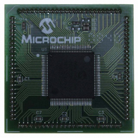
MA330013
Manufacturer Part Number
MA330013
Description
MODULE PLUG-IN DSPIC33 100TQFP
Manufacturer
Microchip Technology
Specifications of MA330013
Accessory Type
Plug-In Module (PIM) - dsPIC33FJ256MC710
Tool / Board Applications
General Purpose MCU, MPU, DSP, DSC
Mcu Supported Families
DsPIC33
Silicon Manufacturer
Microchip
Core Architecture
DsPIC
Core Sub-architecture
DsPIC33
Silicon Core Number
DsPIC33F
Silicon Family Name
DsPIC33FJxxMCxxx
Rohs Compliant
Yes
For Use With
DM330023 - BOARD DEV DSPICDEM MCHV
Lead Free Status / RoHS Status
Not applicable / Not applicable
For Use With/related Products
Explorer 16 (DM240001 or DM240002)
Lead Free Status / RoHS Status
Lead free / RoHS Compliant, Not applicable / Not applicable


REGISTER 4-1:
© 2007 Microchip Technology Inc.
bit 15
bit 7
Legend:
R = Readable bit
-n = Value at POR
bit 15
bit 14
bit 13
bit 12-7
bit 6
bit 5-4
bit 3-0
Note 1:
R/SO-0
WR
U-0
—
2:
(1)
These bits can only be reset on POR.
All other combinations of NVMOP<3:0> are unimplemented.
WR: Write Control bit
1 = Initiates a Flash memory program or erase operation. The operation is self-timed and the bit is
0 = Program or erase operation is complete and inactive
WREN: Write Enable bit
1 = Enable Flash program/erase operations
0 = Inhibit Flash program/erase operations
WRERR: Write Sequence Error Flag bit
1 = An improper program or erase sequence attempt or termination has occurred (bit is set
0 = The program or erase operation completed normally
Unimplemented: Read as ‘0’
ERASE: Erase/Program Enable bit
1 = Perform the erase operation specified by NVMOP<3:0> on the next WR command
0 = Perform the program operation specified by NVMOP<3:0> on the next WR command
Unimplemented: Read as ‘0’
NVMOP<3:0>: NVM Operation Select bits
1111 = Memory bulk erase operation (ERASE = 1) or no operation (ERASE = 0)
1110 = Reserved
1101 = Erase General Segment and FGS Configuration register
1100 = Erase Secure Segment and FSS Configuration register
1011 = Reserved
0011 = Memory word program operation (ERASE = 0) or no operation (ERASE = 1)
0010 = Memory page erase operation (ERASE = 1) or no operation (ERASE = 0)
0001 = Memory row program operation (ERASE = 0) or no operation (ERASE = 1)
0000 = Program or erase a single Configuration register byte
R/W-0
R/W-0
ERASE
WREN
cleared by hardware once operation is complete.
automatically on any set attempt of the WR bit)
NVMCON: FLASH MEMORY CONTROL REGISTER
(ERASE = 1) or no operation (ERASE = 0)
(ERASE = 1) or no operation (ERASE = 0)
(1)
(1)
SO = Satiable only bit
W = Writable bit
‘1’ = Bit is set
R/W-0
WRERR
U-0
—
(1)
U-0
U-0
Preliminary
—
—
(2)
U = Unimplemented bit, read as ‘0’
‘0’ = Bit is cleared
R/W-0
U-0
—
(1)
R/W-0
U-0
—
NVMOP<3:0>
(1)
x = Bit is unknown
R/W-0
dsPIC33F
U-0
(2)
—
(1)
DS70165E-page 79
R/W-0
U-0
—
(1)
bit 8
bit 0
Related parts for MA330013
Image
Part Number
Description
Manufacturer
Datasheet
Request
R

Part Number:
Description:
Manufacturer:
Microchip Technology Inc.
Datasheet:
Part Number:
Description:
Manufacturer:
Microchip Technology Inc.
Datasheet:
Part Number:
Description:
Manufacturer:
Microchip Technology Inc.
Datasheet:
Part Number:
Description:
Manufacturer:
Microchip Technology Inc.
Datasheet:
Part Number:
Description:
Manufacturer:
Microchip Technology Inc.
Datasheet:
Part Number:
Description:
Manufacturer:
Microchip Technology Inc.
Datasheet:
Part Number:
Description:
Manufacturer:
Microchip Technology Inc.
Datasheet:
Part Number:
Description:
Manufacturer:
Microchip Technology Inc.
Datasheet: