MA330013 Microchip Technology, MA330013 Datasheet - Page 235
MA330013
Manufacturer Part Number
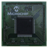
MA330013
Description
MODULE PLUG-IN DSPIC33 100TQFP
Manufacturer
Microchip Technology
Specifications of MA330013
Accessory Type
Plug-In Module (PIM) - dsPIC33FJ256MC710
Tool / Board Applications
General Purpose MCU, MPU, DSP, DSC
Mcu Supported Families
DsPIC33
Silicon Manufacturer
Microchip
Core Architecture
DsPIC
Core Sub-architecture
DsPIC33
Silicon Core Number
DsPIC33F
Silicon Family Name
DsPIC33FJxxMCxxx
Rohs Compliant
Yes
For Use With
DM330023 - BOARD DEV DSPICDEM MCHV
Lead Free Status / RoHS Status
Not applicable / Not applicable
For Use With/related Products
Explorer 16 (DM240001 or DM240002)
Lead Free Status / RoHS Status
Lead free / RoHS Compliant, Not applicable / Not applicable


20.3
The CAN module can operate in one of several operation
modes selected by the user. These modes include:
• Initialization Mode
• Disable Mode
• Normal Operation Mode
• Listen Only Mode
• Listen All Messages Mode
• Loopback Mode
Modes are requested by setting the REQOP<2:0> bits
(CiCTRL1<10:8>). Entry into a mode is Acknowledged
by
(CiCTRL1<7:5>). The module will not change the mode
and the OPMODE bits until a change in mode is
acceptable, generally during bus Idle time, which is
defined as at least 11 consecutive recessive bits.
20.3.1
In the Initialization mode, the module will not transmit or
receive. The error counters are cleared and the inter-
rupt flags remain unchanged. The programmer will
have access to Configuration registers that are access
restricted in other modes. The module will protect the
user from accidentally violating the CAN protocol
through programming errors. All registers which control
the configuration of the module can not be modified
while the module is on-line. The CAN module will not
be allowed to enter the Configuration mode while a
transmission is taking place. The Configuration mode
serves as a lock to protect the following registers:
• All Module Control Registers
• Baud Rate and Interrupt Configuration Registers
• Bus Timing Registers
• Identifier Acceptance Filter Registers
• Identifier Acceptance Mask Registers
20.3.2
In Disable mode, the module will not transmit or
receive. The module has the ability to set the WAKIF bit
due to bus activity, however, any pending interrupts will
remain and the error counters will retain their value.
If the REQOP<2:0> bits (CiCTRL1<10:8>) = 001, the
module will enter the Module Disable mode. If the module
is active, the module will wait for 11 recessive bits on the
CAN bus, detect that condition as an Idle bus, then
accept the module disable command. When the
OPMODE<2:0> bits (CiCTRL1<7:5>) = 001, that indi-
cates whether the module successfully went into Module
Disable mode. The I/O pins will revert to normal I/O
function when the module is in the Module Disable mode.
The module can be programmed to apply a low-pass
filter function to the CiRX input line while the module or
the CPU is in Sleep mode. The WAKFIL bit
(CiCFG2<14>) enables or disables the filter.
© 2007 Microchip Technology Inc.
monitoring
Modes of Operation
INITIALIZATION MODE
DISABLE MODE
the
OPMODE<2:0>
Preliminary
bits
20.3.3
Normal
REQOP<2:0> = 000. In this mode, the module is
activated and the I/O pins will assume the CAN bus
functions. The module will transmit and receive CAN
bus messages via the CiTX and CiRX pins.
20.3.4
If the Listen Only mode is activated, the module on the
CAN bus is passive. The transmitter buffers revert to
the port I/O function. The receive pins remain inputs.
For the receiver, no error flags or Acknowledge signals
are sent. The error counters are deactivated in this
state. The Listen Only mode can be used for detecting
the baud rate on the CAN bus. To use this, it is neces-
sary that there are at least two further nodes that
communicate with each other.
20.3.5
The module can be set to ignore all errors and receive
any message. The Listen All Messages mode is acti-
vated by setting REQOP<2:0> = ‘111’. In this mode,
the data which is in the message assembly buffer, until
the time an error occurred, is copied in the receive
buffer and can be read via the CPU interface.
20.3.6
If the Loopback mode is activated, the module will con-
nect the internal transmit signal to the internal receive
signal at the module boundary. The transmit and
receive pins revert to their port I/O function.
20.4
20.4.1
The CAN bus module has up to 32 receive buffers,
located in DMA RAM. The first 8 buffers need to be
configured as receive buffers by clearing the
corresponding TX/RX buffer selection (TXENn) bit in a
CiTRmnCON register. The overall size of the CAN
buffer area in DMA RAM is selectable by the user and
is
(CiFCTRL<15:13>). The first 16 buffers can be
assigned to receive filters, while the rest can be used
only as a FIFO buffer.
Note:
defined
Message Reception
Operation
Typically, if the CAN module is allowed to
transmit in a particular mode of operation
and a transmission is requested immedi-
ately after the CAN module has been
placed in that mode of operation, the mod-
ule waits for 11 consecutive recessive bits
on the bus before starting transmission. If
the user switches to Disable mode within
this 11-bit period, then this transmission is
aborted and the corresponding TXABT bit
is set and TXREQ bit is cleared.
NORMAL OPERATION MODE
LISTEN ONLY MODE
LISTEN ALL MESSAGES MODE
LOOPBACK MODE
RECEIVE BUFFERS
by
mode
the
dsPIC33F
is
DMABS<2:0>
DS70165E-page 233
selected
when
bits
Related parts for MA330013
Image
Part Number
Description
Manufacturer
Datasheet
Request
R

Part Number:
Description:
Manufacturer:
Microchip Technology Inc.
Datasheet:
Part Number:
Description:
Manufacturer:
Microchip Technology Inc.
Datasheet:
Part Number:
Description:
Manufacturer:
Microchip Technology Inc.
Datasheet:
Part Number:
Description:
Manufacturer:
Microchip Technology Inc.
Datasheet:
Part Number:
Description:
Manufacturer:
Microchip Technology Inc.
Datasheet:
Part Number:
Description:
Manufacturer:
Microchip Technology Inc.
Datasheet:
Part Number:
Description:
Manufacturer:
Microchip Technology Inc.
Datasheet:
Part Number:
Description:
Manufacturer:
Microchip Technology Inc.
Datasheet: