MA330013 Microchip Technology, MA330013 Datasheet - Page 266
MA330013
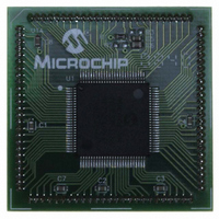
Manufacturer Part Number
MA330013
Description
MODULE PLUG-IN DSPIC33 100TQFP
Manufacturer
Microchip Technology
Specifications of MA330013
Accessory Type
Plug-In Module (PIM) - dsPIC33FJ256MC710
Tool / Board Applications
General Purpose MCU, MPU, DSP, DSC
Mcu Supported Families
DsPIC33
Silicon Manufacturer
Microchip
Core Architecture
DsPIC
Core Sub-architecture
DsPIC33
Silicon Core Number
DsPIC33F
Silicon Family Name
DsPIC33FJxxMCxxx
Rohs Compliant
Yes
For Use With
DM330023 - BOARD DEV DSPICDEM MCHV
Lead Free Status / RoHS Status
Not applicable / Not applicable
For Use With/related Products
Explorer 16 (DM240001 or DM240002)
Lead Free Status / RoHS Status
Lead free / RoHS Compliant, Not applicable / Not applicable


dsPIC33F
21.3.6
When the DCI module is operating as a frame sync
slave (COFSD = 1), data transfers are controlled by the
Codec device attached to the DCI module. The
COFSM control bits control how the DCI module
responds to incoming COFS signals.
In the Multi-Channel mode, a new data frame transfer
will begin one CSCK cycle after the COFS pin is sam-
pled high (see Figure 21-2). The pulse on the COFS
pin resets the frame sync generator logic.
In the I
one CSCK cycle after a low-to-high or a high-to-low
transition is sampled on the COFS pin. A rising or fall-
ing edge on the COFS pin resets the frame sync
generator logic.
FIGURE 21-2:
FIGURE 21-3:
FIGURE 21-4:
DS70165E-page 264
Note:
2
S mode, a new data word will be transferred
SLAVE FRAME SYNC OPERATION
A 5-bit transfer is shown here for illustration purposes. The I
will be system dependent.
CSDO or CSDI
CSDI or CSDO
CSDI/CSDO
BIT_CLK
FRAME SYNC TIMING, MULTI-CHANNEL MODE
FRAME SYNC TIMING, AC-LINK START-OF-FRAME
I
2
CSCK
COFS
SYNC
S INTERFACE FRAME SYNC TIMING
CSCK
WS
MSb
MSb
bit 2
S12
bit 1
S12
Preliminary
S12
LSb
MSb
Tag
In the AC-Link mode, the tag slot and subsequent data
slots for the next frame will be transferred one CSCK
cycle after the COFS pin is sampled high.
The COFSG and WS bits must be configured to pro-
vide the proper frame length when the module is oper-
ating in the Slave mode. Once a valid frame sync pulse
has been sampled by the module on the COFS pin, an
entire data frame transfer will take place. The module
will not respond to further frame sync pulses until the
data frame transfer has completed.
bit 14
LSb MSb
Tag
2
S protocol does not specify word length – this
bit 13
Tag
LSb
© 2007 Microchip Technology Inc.
LSb
Related parts for MA330013
Image
Part Number
Description
Manufacturer
Datasheet
Request
R

Part Number:
Description:
Manufacturer:
Microchip Technology Inc.
Datasheet:
Part Number:
Description:
Manufacturer:
Microchip Technology Inc.
Datasheet:
Part Number:
Description:
Manufacturer:
Microchip Technology Inc.
Datasheet:
Part Number:
Description:
Manufacturer:
Microchip Technology Inc.
Datasheet:
Part Number:
Description:
Manufacturer:
Microchip Technology Inc.
Datasheet:
Part Number:
Description:
Manufacturer:
Microchip Technology Inc.
Datasheet:
Part Number:
Description:
Manufacturer:
Microchip Technology Inc.
Datasheet:
Part Number:
Description:
Manufacturer:
Microchip Technology Inc.
Datasheet: