C8051F320DK Silicon Laboratories Inc, C8051F320DK Datasheet - Page 114
C8051F320DK
Manufacturer Part Number
C8051F320DK
Description
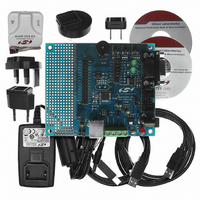
DEV KIT FOR C8051F320/F321
Manufacturer
Silicon Laboratories Inc
Type
MCUr
Specifications of C8051F320DK
Contents
Evaluation Board, Power Supply, USB Cables, Adapter and Documentation
Processor To Be Evaluated
C8051F320/F321
Interface Type
USB
Silicon Manufacturer
Silicon Labs
Core Architecture
8051
Silicon Core Number
C8051F320
Silicon Family Name
C8051F32x
Lead Free Status / RoHS Status
Contains lead / RoHS non-compliant
For Use With/related Products
Silicon Laboratories C8051F320, C8051F321
Lead Free Status / Rohs Status
Lead free / RoHS Compliant
Other names
336-1260
Available stocks
Company
Part Number
Manufacturer
Quantity
Price
Company:

Part Number:
C8051F320DK
Manufacturer:
SiliconL
Quantity:
4


C8051F320/1
12. External RAM
The C8051F320/1 devices include 2048 bytes of on-chip XRAM. This XRAM space is split into user RAM
(addresses 0x0000 - 0x03FF) and USB0 FIFO space (addresses 0x0400 - 0x07FF).
12.1. Accessing User XRAM
XRAM can be accessed using the external move instruction (MOVX) and the data pointer (DPTR), or using
MOVX indirect addressing mode. If the MOVX instruction is used with an 8-bit address operand (such as
@R1), then the high byte of the 16-bit address is provided by the External Memory Interface Control Reg-
ister (EMI0CN as shown in Figure 12.1). Note: the MOVX instruction is also used for writes to the Flash
memory. See Section “11. Flash Memory” on page 106 for details. The MOVX instruction accesses XRAM
by default.
For any of the addressing modes the upper 5 bits of the 16-bit external data memory address word are
"don't cares". As a result, the 2048-byte RAM is mapped modulo style over the entire 64k external data
memory address range. For example, the XRAM byte at address 0x0000 is also at address 0x0800,
0x1000, 0x1800, 0x2000, etc.
Important Note: The upper 1k of the 2k XRAM functions as USB FIFO space. See Section 12.2 for
details on accessing this memory space.
12.2. Accessing USB FIFO Space
The upper 1k of XRAM functions as USB FIFO space. Figure 12.2 shows an expanded view of the FIFO
space and user XRAM. FIFO space is accessed via USB FIFO registers; see Section “15.5. FIFO Manage-
ment” on page 147 for more information on accessing these FIFOs. The MOVX instruction should not be
used to load or modify USB data in the FIFO space.
Unused areas of the FIFO space may be used as general purpose XRAM, accessible as described in Sec-
tion 12.1. The FIFO block operates on the USB clock domain; thus the USB clock must be active when
accessing FIFO space. Note that the number of SYSCLK cycles required by the MOVX instruction is
increased when accessing USB FIFO space.
Important Note: The USB clock must be active when accessing FIFO space.
114
0xFFFF
0x07FF
0x03FF
0x0800
0x0400
0x0000
Figure 12.1. External Ram Memory Map
0x0000 to 0x07FF, wrapped
Same 2048 bytes as from
on 2 kB boundaries
USB FIFOs
1024 Bytes
1024 Bytes
XRAM
Rev. 1.4
Accessed through USB FIFO
registers
Accessed with the MOVX
instruction
Related parts for C8051F320DK
Image
Part Number
Description
Manufacturer
Datasheet
Request
R

Part Number:
Description:
SMD/C°/SINGLE-ENDED OUTPUT SILICON OSCILLATOR
Manufacturer:
Silicon Laboratories Inc
Part Number:
Description:
Manufacturer:
Silicon Laboratories Inc
Datasheet:
Part Number:
Description:
N/A N/A/SI4010 AES KEYFOB DEMO WITH LCD RX
Manufacturer:
Silicon Laboratories Inc
Datasheet:
Part Number:
Description:
N/A N/A/SI4010 SIMPLIFIED KEY FOB DEMO WITH LED RX
Manufacturer:
Silicon Laboratories Inc
Datasheet:
Part Number:
Description:
N/A/-40 TO 85 OC/EZLINK MODULE; F930/4432 HIGH BAND (REV E/B1)
Manufacturer:
Silicon Laboratories Inc
Part Number:
Description:
EZLink Module; F930/4432 Low Band (rev e/B1)
Manufacturer:
Silicon Laboratories Inc
Part Number:
Description:
I°/4460 10 DBM RADIO TEST CARD 434 MHZ
Manufacturer:
Silicon Laboratories Inc
Part Number:
Description:
I°/4461 14 DBM RADIO TEST CARD 868 MHZ
Manufacturer:
Silicon Laboratories Inc
Part Number:
Description:
I°/4463 20 DBM RFSWITCH RADIO TEST CARD 460 MHZ
Manufacturer:
Silicon Laboratories Inc
Part Number:
Description:
I°/4463 20 DBM RADIO TEST CARD 868 MHZ
Manufacturer:
Silicon Laboratories Inc
Part Number:
Description:
I°/4463 27 DBM RADIO TEST CARD 868 MHZ
Manufacturer:
Silicon Laboratories Inc
Part Number:
Description:
I°/4463 SKYWORKS 30 DBM RADIO TEST CARD 915 MHZ
Manufacturer:
Silicon Laboratories Inc
Part Number:
Description:
N/A N/A/-40 TO 85 OC/4463 RFMD 30 DBM RADIO TEST CARD 915 MHZ
Manufacturer:
Silicon Laboratories Inc
Part Number:
Description:
I°/4463 20 DBM RADIO TEST CARD 169 MHZ
Manufacturer:
Silicon Laboratories Inc