C8051F320DK Silicon Laboratories Inc, C8051F320DK Datasheet - Page 141
C8051F320DK
Manufacturer Part Number
C8051F320DK
Description
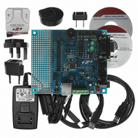
DEV KIT FOR C8051F320/F321
Manufacturer
Silicon Laboratories Inc
Type
MCUr
Specifications of C8051F320DK
Contents
Evaluation Board, Power Supply, USB Cables, Adapter and Documentation
Processor To Be Evaluated
C8051F320/F321
Interface Type
USB
Silicon Manufacturer
Silicon Labs
Core Architecture
8051
Silicon Core Number
C8051F320
Silicon Family Name
C8051F32x
Lead Free Status / RoHS Status
Contains lead / RoHS non-compliant
For Use With/related Products
Silicon Laboratories C8051F320, C8051F321
Lead Free Status / Rohs Status
Lead free / RoHS Compliant
Other names
336-1260
Available stocks
Company
Part Number
Manufacturer
Quantity
Price
Company:

Part Number:
C8051F320DK
Manufacturer:
SiliconL
Quantity:
4


Bit7:
Bit6:
Bit5:
Bits4–3: PHYTST1–0: Physical Layer Test
Bit2:
Bit1:
Bit0:
PREN
R/W
Bit7
PREN: Internal Pull-up Resistor Enable
The location of the pull-up resistor (D+ or D–) is determined by the SPEED bit.
0: Internal pull-up resistor disabled (device effectively detached from the USB network).
1: Internal pull-up resistor enabled when VBUS is present (device attached to the USB net-
work).
PHYEN: Physical Layer Enable
This bit enables/disables the USB0 physical layer transceiver.
0: Transceiver disabled (suspend).
1: Transceiver enabled (normal).
SPEED: USB0 Speed Select
This bit selects the USB0 speed.
0: USB0 operates as a Low Speed device. If enabled, the internal pull-up resistor appears
on the D– line.
1: USB0 operates as a Full Speed device. If enabled, the internal pull-up resistor appears on
the D+ line.
These bits can be used to test the USB0 transceiver.
DFREC: Differential Receiver
The state of this bit indicates the current differential value present on the D+ and D– lines
when PHYEN = ‘1’.
0: Differential ‘0’ signaling on the bus.
1: Differential ‘1’ signaling on the bus.
Dp: D+ Signal Status
This bit indicates the current logic level of the D+ pin.
0: D+ signal currently at logic 0.
1: D+ signal currently at logic 1.
Dn: D- Signal Status
This bit indicates the current logic level of the D– pin.
0: D– signal currently at logic 0.
1: D– signal currently at logic 1.
PHYTST[1:0]
PHYEN
SFR Definition 15.1. USB0XCN: USB0 Transceiver Control
R/W
Bit6
00b
01b
10b
11b
SPEED
R/W
Bit5
Mode 0: Normal (non-test mode)
Mode 1: Differential ‘1’ Forced
Mode 2: Differential ‘0’ Forced
Mode 3: Single-Ended ‘0’ Forced
PHYTST1 PHYTST0 DFREC
R/W
Bit4
Mode
Rev. 1.4
R/W
Bit3
Bit2
R
D+
X
1
0
0
D–
X
0
1
0
Dp
Bit1
R
C8051F320/1
Bit0
Dn
R
SFR Address:
00000000
Reset Value
0xD7
141
Related parts for C8051F320DK
Image
Part Number
Description
Manufacturer
Datasheet
Request
R

Part Number:
Description:
SMD/C°/SINGLE-ENDED OUTPUT SILICON OSCILLATOR
Manufacturer:
Silicon Laboratories Inc
Part Number:
Description:
Manufacturer:
Silicon Laboratories Inc
Datasheet:
Part Number:
Description:
N/A N/A/SI4010 AES KEYFOB DEMO WITH LCD RX
Manufacturer:
Silicon Laboratories Inc
Datasheet:
Part Number:
Description:
N/A N/A/SI4010 SIMPLIFIED KEY FOB DEMO WITH LED RX
Manufacturer:
Silicon Laboratories Inc
Datasheet:
Part Number:
Description:
N/A/-40 TO 85 OC/EZLINK MODULE; F930/4432 HIGH BAND (REV E/B1)
Manufacturer:
Silicon Laboratories Inc
Part Number:
Description:
EZLink Module; F930/4432 Low Band (rev e/B1)
Manufacturer:
Silicon Laboratories Inc
Part Number:
Description:
I°/4460 10 DBM RADIO TEST CARD 434 MHZ
Manufacturer:
Silicon Laboratories Inc
Part Number:
Description:
I°/4461 14 DBM RADIO TEST CARD 868 MHZ
Manufacturer:
Silicon Laboratories Inc
Part Number:
Description:
I°/4463 20 DBM RFSWITCH RADIO TEST CARD 460 MHZ
Manufacturer:
Silicon Laboratories Inc
Part Number:
Description:
I°/4463 20 DBM RADIO TEST CARD 868 MHZ
Manufacturer:
Silicon Laboratories Inc
Part Number:
Description:
I°/4463 27 DBM RADIO TEST CARD 868 MHZ
Manufacturer:
Silicon Laboratories Inc
Part Number:
Description:
I°/4463 SKYWORKS 30 DBM RADIO TEST CARD 915 MHZ
Manufacturer:
Silicon Laboratories Inc
Part Number:
Description:
N/A N/A/-40 TO 85 OC/4463 RFMD 30 DBM RADIO TEST CARD 915 MHZ
Manufacturer:
Silicon Laboratories Inc
Part Number:
Description:
I°/4463 20 DBM RADIO TEST CARD 169 MHZ
Manufacturer:
Silicon Laboratories Inc