C8051F320DK Silicon Laboratories Inc, C8051F320DK Datasheet - Page 227
C8051F320DK
Manufacturer Part Number
C8051F320DK
Description
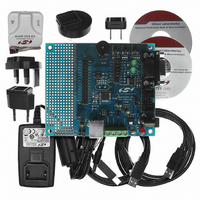
DEV KIT FOR C8051F320/F321
Manufacturer
Silicon Laboratories Inc
Type
MCUr
Specifications of C8051F320DK
Contents
Evaluation Board, Power Supply, USB Cables, Adapter and Documentation
Processor To Be Evaluated
C8051F320/F321
Interface Type
USB
Silicon Manufacturer
Silicon Labs
Core Architecture
8051
Silicon Core Number
C8051F320
Silicon Family Name
C8051F32x
Lead Free Status / RoHS Status
Contains lead / RoHS non-compliant
For Use With/related Products
Silicon Laboratories C8051F320, C8051F321
Lead Free Status / Rohs Status
Lead free / RoHS Compliant
Other names
336-1260
Available stocks
Company
Part Number
Manufacturer
Quantity
Price
Company:

Part Number:
C8051F320DK
Manufacturer:
SiliconL
Quantity:
4


20. Programmable Counter Array (PCA0)
The Programmable Counter Array (PCA0) provides enhanced timer functionality while requiring less CPU
intervention than the standard 8051 counter/timers. The PCA consists of a dedicated 16-bit counter/timer
and five 16-bit capture/compare modules. Each capture/compare module has its own associated I/O line
(CEXn) which is routed through the Crossbar to Port I/O when enabled (See Section “14.1. Priority Cross-
bar Decoder” on page 128 for details on configuring the Crossbar). The counter/timer is driven by a pro-
grammable timebase that can select between six sources: system clock, system clock divided by four,
system clock divided by twelve, the external oscillator clock source divided by 8, Timer 0 overflow, or an
external clock signal on the ECI input pin. Each capture/compare module may be configured to operate
independently in one of six modes: Edge-Triggered Capture, Software Timer, High-Speed Output, Fre-
quency Output, 8-Bit PWM, or 16-Bit PWM (each mode is described in Section “20.2. Capture/Compare
Modules” on page 229). The external oscillator clock option is ideal for real-time clock (RTC) functionality,
allowing the PCA to be clocked by a precision external oscillator while the internal oscillator drives the sys-
tem clock. The PCA is configured and controlled through the system controller's Special Function Regis-
ters. The PCA block diagram is shown in Figure 20.1.
Note: The PCA Module 4 may be used as a watchdog timer (WDT), and is enabled in this mode following a system
reset. Access to certain PCA registers is restricted while WDT mode is enabled. See Section 20.3 for details
Capture/Compare
Module 0
SYSCLK/12
Timer 0 Overflow
SYSCLK
External Clock/8
SYSCLK/4
ECI
Figure 20.1. PCA Block Diagram
Capture/Compare
Module 1
CLOCK
MUX
PCA
Crossbar
16-Bit Counter/Timer
Port I/O
Rev. 1.4
Capture/Compare
Module 2
Capture/Compare
Module 3
C8051F320/1
Capture/Compare
Module 4 / WDT
227
Related parts for C8051F320DK
Image
Part Number
Description
Manufacturer
Datasheet
Request
R

Part Number:
Description:
SMD/C°/SINGLE-ENDED OUTPUT SILICON OSCILLATOR
Manufacturer:
Silicon Laboratories Inc
Part Number:
Description:
Manufacturer:
Silicon Laboratories Inc
Datasheet:
Part Number:
Description:
N/A N/A/SI4010 AES KEYFOB DEMO WITH LCD RX
Manufacturer:
Silicon Laboratories Inc
Datasheet:
Part Number:
Description:
N/A N/A/SI4010 SIMPLIFIED KEY FOB DEMO WITH LED RX
Manufacturer:
Silicon Laboratories Inc
Datasheet:
Part Number:
Description:
N/A/-40 TO 85 OC/EZLINK MODULE; F930/4432 HIGH BAND (REV E/B1)
Manufacturer:
Silicon Laboratories Inc
Part Number:
Description:
EZLink Module; F930/4432 Low Band (rev e/B1)
Manufacturer:
Silicon Laboratories Inc
Part Number:
Description:
I°/4460 10 DBM RADIO TEST CARD 434 MHZ
Manufacturer:
Silicon Laboratories Inc
Part Number:
Description:
I°/4461 14 DBM RADIO TEST CARD 868 MHZ
Manufacturer:
Silicon Laboratories Inc
Part Number:
Description:
I°/4463 20 DBM RFSWITCH RADIO TEST CARD 460 MHZ
Manufacturer:
Silicon Laboratories Inc
Part Number:
Description:
I°/4463 20 DBM RADIO TEST CARD 868 MHZ
Manufacturer:
Silicon Laboratories Inc
Part Number:
Description:
I°/4463 27 DBM RADIO TEST CARD 868 MHZ
Manufacturer:
Silicon Laboratories Inc
Part Number:
Description:
I°/4463 SKYWORKS 30 DBM RADIO TEST CARD 915 MHZ
Manufacturer:
Silicon Laboratories Inc
Part Number:
Description:
N/A N/A/-40 TO 85 OC/4463 RFMD 30 DBM RADIO TEST CARD 915 MHZ
Manufacturer:
Silicon Laboratories Inc
Part Number:
Description:
I°/4463 20 DBM RADIO TEST CARD 169 MHZ
Manufacturer:
Silicon Laboratories Inc