C8051F320DK Silicon Laboratories Inc, C8051F320DK Datasheet - Page 211
C8051F320DK
Manufacturer Part Number
C8051F320DK
Description
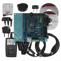
DEV KIT FOR C8051F320/F321
Manufacturer
Silicon Laboratories Inc
Type
MCUr
Specifications of C8051F320DK
Contents
Evaluation Board, Power Supply, USB Cables, Adapter and Documentation
Processor To Be Evaluated
C8051F320/F321
Interface Type
USB
Silicon Manufacturer
Silicon Labs
Core Architecture
8051
Silicon Core Number
C8051F320
Silicon Family Name
C8051F32x
Lead Free Status / RoHS Status
Contains lead / RoHS non-compliant
For Use With/related Products
Silicon Laboratories C8051F320, C8051F321
Lead Free Status / Rohs Status
Lead free / RoHS Compliant
Other names
336-1260
Available stocks
Company
Part Number
Manufacturer
Quantity
Price
Company:

Part Number:
C8051F320DK
Manufacturer:
SiliconL
Quantity:
4


19.1.2. Mode 1: 16-bit Counter/Timer
Mode 1 operation is the same as Mode 0, except that the counter/timer registers use all 16 bits. The coun-
ter/timers are enabled and configured in Mode 1 in the same manner as for Mode 0.
19.1.3. Mode 2: 8-bit Counter/Timer with Auto-Reload
Mode 2 configures Timer 0 and Timer 1 to operate as 8-bit counter/timers with automatic reload of the start
value. TL0 holds the count and TH0 holds the reload value. When the counter in TL0 overflows from all
ones to 0x00, the timer overflow flag TF0 (TCON.5) is set and the counter in TL0 is reloaded from TH0. If
Timer 0 interrupts are enabled, an interrupt will occur when the TF0 flag is set. The reload value in TH0 is
not changed. TL0 must be initialized to the desired value before enabling the timer for the first count to be
correct. When in Mode 2, Timer 1 operates identically to Timer 0.
Both counter/timers are enabled and configured in Mode 2 in the same manner as Mode 0. Setting the
TR0 bit (TCON.4) enables the timer when either GATE0 (TMOD.3) is logic 0 or when the input signal /INT0
is active as defined by bit IN0PL in register INT01CF (see Section “9.3.2. External Interrupts” on page 88
for details on the external input signals /INT0 and /INT1).
/INT0
T0
Crossbar
Pre-scaled Clock
SYSCLK
IN0PL
GATE0
Figure 19.2. T0 Mode 2 Block Diagram
XOR
0
1
TR0
M
H
T
3
M
T
3
L
CKCON
M
H
T
2
M
T
2
L
0
1
M
T
1
M
T
0
C
S
A
1
Rev. 1.4
C
S
A
0
G
A
T
E
1
C
T
1
/
M
T
1
1
TMOD
M
T
1
0
TCLK
G
A
T
E
0
C
T
0
/
M
T
0
1
M
T
0
0
(8 bits)
(8 bits)
TH0
TL0
N
P
1
L
I
N
S
1
L
2
I
INT01CF
N
1
S
L
1
I
N
1
S
L
0
I
N
P
0
L
I
Reload
N
0
S
L
2
I
N
0
S
L
1
I
N
0
S
L
0
I
C8051F320/1
TR1
TR0
TF1
TF0
IE1
IT1
IE0
IT0
Interrupt
211
Related parts for C8051F320DK
Image
Part Number
Description
Manufacturer
Datasheet
Request
R

Part Number:
Description:
SMD/C°/SINGLE-ENDED OUTPUT SILICON OSCILLATOR
Manufacturer:
Silicon Laboratories Inc
Part Number:
Description:
Manufacturer:
Silicon Laboratories Inc
Datasheet:
Part Number:
Description:
N/A N/A/SI4010 AES KEYFOB DEMO WITH LCD RX
Manufacturer:
Silicon Laboratories Inc
Datasheet:
Part Number:
Description:
N/A N/A/SI4010 SIMPLIFIED KEY FOB DEMO WITH LED RX
Manufacturer:
Silicon Laboratories Inc
Datasheet:
Part Number:
Description:
N/A/-40 TO 85 OC/EZLINK MODULE; F930/4432 HIGH BAND (REV E/B1)
Manufacturer:
Silicon Laboratories Inc
Part Number:
Description:
EZLink Module; F930/4432 Low Band (rev e/B1)
Manufacturer:
Silicon Laboratories Inc
Part Number:
Description:
I°/4460 10 DBM RADIO TEST CARD 434 MHZ
Manufacturer:
Silicon Laboratories Inc
Part Number:
Description:
I°/4461 14 DBM RADIO TEST CARD 868 MHZ
Manufacturer:
Silicon Laboratories Inc
Part Number:
Description:
I°/4463 20 DBM RFSWITCH RADIO TEST CARD 460 MHZ
Manufacturer:
Silicon Laboratories Inc
Part Number:
Description:
I°/4463 20 DBM RADIO TEST CARD 868 MHZ
Manufacturer:
Silicon Laboratories Inc
Part Number:
Description:
I°/4463 27 DBM RADIO TEST CARD 868 MHZ
Manufacturer:
Silicon Laboratories Inc
Part Number:
Description:
I°/4463 SKYWORKS 30 DBM RADIO TEST CARD 915 MHZ
Manufacturer:
Silicon Laboratories Inc
Part Number:
Description:
N/A N/A/-40 TO 85 OC/4463 RFMD 30 DBM RADIO TEST CARD 915 MHZ
Manufacturer:
Silicon Laboratories Inc
Part Number:
Description:
I°/4463 20 DBM RADIO TEST CARD 169 MHZ
Manufacturer:
Silicon Laboratories Inc